From Sand to Silicon: ASICs and FPGAs Explained
Tomas Choi and Johnny Martinez
October 29th, 2023
If I asked you to think of some electronic devices, what comes to mind? Most people would probably say something along the lines of "laptops," "PCs," and "smartphones." These everyday gadgets have become integral parts of our lives, and we interact with them constantly. But have you ever wondered what enables these devices to do what they do? The answer lies in the intricate world of semiconductors, and two key players within that world are Field-Programmable Gate Arrays (FPGAs) and Application-Specific Integrated Circuits (ASICs).
In this blog post, we are going to pull back the curtain, and explain a bit more about what FPGAs and ASICs are, and why they are so important.
What is Digital Logic
All computers work by processing a bunch of data in the form of ones and zeros. In digital electronics, we refer to these ones and zeros as bits. A bit can either be one or zero at a given time. On these bits, you can perform numerous logical operations using logic gates. We visualize the output of these logical operations as truth tables, which tell us the expected output given two bits at any given state. See the graphic below.
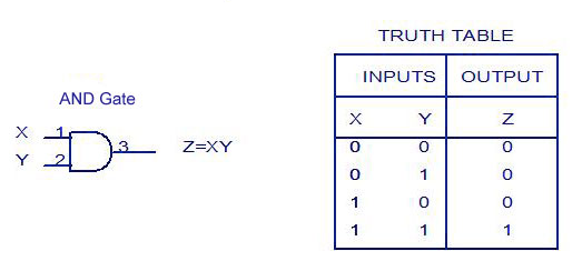
For example, if I had bits X and Y, holding states one and zero respectively, and I performed the AND operation on them, the expected output is zero. An AND gate is just one example of the many logical operations/gates that exist. Each operation/gate has rather simple, well defined behavior, but when combined, are a powerful tool. With them, we can construct complex logical expressions that allow us to build computers, microprocessors, microcontrollers, etc.
What is an FPGA?
Recall, FPGA stands for Field Programmable Gate Arrays. Believe it or not, the name is rather intuitive. An FPGA is an assortment of millions of different logic gates constructed into groupings called logic elements. The programmer can connect these logic elements though a hardware description language (HDL) such as Verilog or VHDL. On C2S2, we use Verilog, but other designers have their own preferences. FPGA vendors typically provide closed-source IP blocks to accelerate the development process and make it easier for designers to implement complex functions in their FPGA-based designs. They can help save time and effort, as designers don't need to create these components from scratch. Furthermore, their functionality has already been verified by the vendor. However, because they are closed-source, the internal details and source code of these IP blocks are not accessible or modifiable by the designers. Onboard memory components, such as RAM and flash memory, are also frequently integrated into FPGAs. These memory resources are essential for storing data and program code, and they can be critical for the performance and functionality of FPGA-based applications.
FPGA Design Flow
The first step in programming an FPGA is implementing your design. As I mentioned before, FPGAs are basically just an assortment of gates; we need to tell the FPGA how to configure these gates. To do this, we write code in our preferred HDL. These HDLs allow us to represent combinations of gates though words and operators. For example, if I wanted to perform the AND operation on bits X and Y in Verilog, I could use the & operator. See the code snippet below.
logic X;logic Y;
logic result;
assign X = 1;
assign Y = 0;
assign result = X & Y;
Once a designer finishes their implementation, they must synthesize their design. Synthesis is the process in which the register transfer level (RTL) design is converted into a gate-level netlist, a representation of the digital circuit using gates and flip-flops (a storage element). FPGA vendors provide software in their IDEs that take care of the Synthesis stage. As a matter of fact, vendors provide software to take care of the remaining steps in the design process. After synthesis, the design goes through Place and Route (PnR). During placement, the optimal physical arrangement of logic elements on the chip's surface is determined, taking into account performance, power, and space constraints. Subsequently, routing controls the interconnections and wiring paths, ensuring efficient signal propagation and adhering to design specifications. Once the PnR is completed, the final step is to generate the bitstream. This step generates a binary file (the bitstream) that encodes the configuration of the FPGA, specifying which logic elements are activated, how they are interconnected, and the values of various configuration bits. Now that we have generated our bitstream, we can flash it to our FPGA, and observe if our design runs. It is also good practice to conduct simulation testing on our designs as well. This step allows you to simulate the hardware's behavior, and can be used to ensure the functionality of a design by conducting tests.
What is an ASIC?
Application Specific Integrated Circuits, or ASICs for short, have become more popular in the evolving semiconductor industry and they now play a pivotal role in numerous technological domains. Unlike general purpose processors that can handle a variety of tasks, ASICs are designed to perform specific functions with unparalleled efficiency and precision. The idea of an ASIC came about in order to keep up with the ever growing demands for better performance. ASICs allow you to achieve an invaluable performance optimization since it only needs to excel at executing a singular task. With a streamlined design that eliminates unnecessary components, ASICs also consume less power compared to general purpose processors.
However, designing an ASIC has its complexities and challenges. Engineers need to be well-versed in hardware description languages and the intricacies of semiconductor technology. Understanding the nuances of the application and how to optimize the design for it is critical because that is where ASICs shine in comparison to general purpose chips. There is also a long timeline that results from multiple phases, including RTL coding, verification, synthesis, place and route, power analysis, fabrication, and testing. Each of these steps involves meticulous planning, design, and rigorous testing to ensure the ASIC functions as intended. Any hiccup in this extended timeline could impact project schedules and budgets.
The world of ASICs is a complex and intricate one, but the rewards are significant. ASICs have the potential to deliver unmatched performance, power efficiency, and cost savings in the right applications, providing favorable trade offs. Also, there are an increasing number of open source hardware tools that can be used to facilitate the entire design flow. C2S2 leverages these open source hardware tools to allow anyone with the creativity and passion in chip design to fulfill this complex but rewarding task.
FPGA vs. ASIC
FPGAs and ASICs are both critical components in the world of digital design, but they serve different purposes and have unique characteristics. ASICs are tailor-made for specific applications. This customization allows ASICs to excel in dedicated tasks, providing the highest performance and power efficiency. ASICs are also smaller and consume less power compared to FPGAs. On the other hand, FPGAs are highly flexible and can be reprogrammed to perform various tasks. Their architecture consists of programmable logic gates, allowing designers to change the functionality of the chip as needed. FPGAs are excellent for rapid prototyping and iterative development. Engineers can experiment with different designs without the high costs and long lead times associated with ASIC development. Both technologies have their advantages, and these clearly depict why they are so prevalent in the semiconductor industry. Everyone's fascination with FPGAs and ASICs stems from their role as the foundation upon which our modern world of electronics and computing is built, enabling breakthroughs, efficiency, and customization that drive technological progress.