PCB Design: "There's Layers To It"
Chimdi Anude and Sherri Qazi
December 3rd, 2023
One of the main jobs of System Architecture is developing Printed Circuit Boards (PCBs) to host our silicon chips. However, starting one is not as simple as opening up Altium Designer or any design software of your choice on your laptop, placing parts and drawing wires. There are preliminary steps to be taken to ensure success and to make route your board a lot easier. So we are going to show the "layers" on what goes on in PCB Design.
The biggest first step is knowing what components you want/need on your board and making a power tree for it. A power tree is a diagram that shows the power distributed throughout the system. For the PCB that hosted the chip made from the class our Faculty Advisor teaches (ECE 5745 Complex Digital ASIC Design), the integrated circuits (ICs) we had to consider were a clock (10MHz to be exact), flash memory, a MCP module and a LED. Also the input and output (I/O) pins of the chip itself. Checking the datasheet for these ICs are important because they rely on what the input voltage it can handle.
We chose to use a USB module because it can deliver both power and data and delivers about 5V. So that is the root of our power tree.From there, the most common input voltages ICs have are either 1.8V or 3.3V. We can step down the voltage by using what is called a Low Dropout Regulator (LDO). We choose this to regulate our voltage because we are focused on building a low power system and the voltage difference between the input and output are small. We draw two arrows from the USB to the two LDOs. From there we can sort our ICs, to take either 1.8V, 3.3V or 5V. For this particular board. As seen in the diagram below, the MCP is directly connected to the USB module, taking 5V as an input, for 3.3V one of the LDO is connected to flash memory, the clock, LED and some of the I/O pins. For 1.8V, the other LDO has some of the other I/O pins of the chip as outputs.
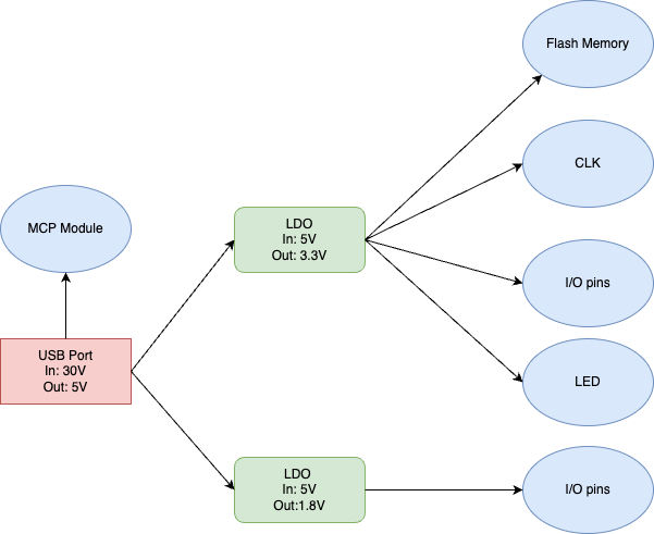
Power Distribution
Another important aspect of PCB design is ensuring that components that you choose for your design are available by the manufacturers of those components and that those components are from one supplier. By having one supplier for the parts, in our case Digikey, we can standardize our board and make it more cohesive. Before placing any random component on a schematic, you first have to look at the specifications of the component and make sure that they meet voltage or current ratings for the surrounding electrical components in your circuit that you're building. For example, when choosing capacitors for an LDO, you want to take note of the capacitor's capacitance, voltage rating, ripple current rating, temperature, etc. The physical size of a capacitor depends on the capacitance value and the voltage rating. Therefore, as the capacitance increases, the size becomes larger.
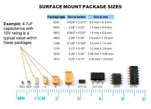
Component Package Sizes
As you can see from the picture above, the package type number increases as the size of the capacitor increases. Generally, we want to keep the package size of capacitors to be on the smaller end because it will give you more space to fit more components on the PCB, have lower inductance, and will most likely be cheaper.
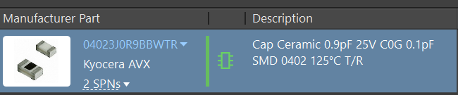
Another important factor when choosing components is to check if the item is in stock. It would be unfortunate to design a PCB just for a part to not be available. In Altium, using the manufacturer part search panel, you can directly search for a part and find what supplier has that particular component available in stock. If the part is low in stock, the green icon below would be orange, and if the part is out of stock the part symbol would be red. You can also look directly at the supplier's website and search for the part there.
Once you have confirmed the part's stock and specifications, you can finally place the part on the schematic. PCB design with careful planning can save you time and the hassle of replacing parts and altering your schematic in order to have a functional board. That's why it's important to consider all possibilities or "layers" when designing your board.