The Analog Subteam Process Flow
Thomas Figura and David Bertuch
October 15th, 2023
To properly tape out an analog integrated circuit, one needs to know how to make their way through the analog tape out flow, so we want to share the processes that we used in last year's tape out.
For this blog post, we will go through the process flow of a simple inverter circuit in the SKY130 PDK through the use of XSCHEM/NGSpice, Magic VLSI, and Netgen. We use XSCHEM for the schematic capture and SPICE testing, Magic VLSI for laying out the schematic into metal, and Netgen to check whether the schematic netlist from XSCHEM matches the netlist from Magic.
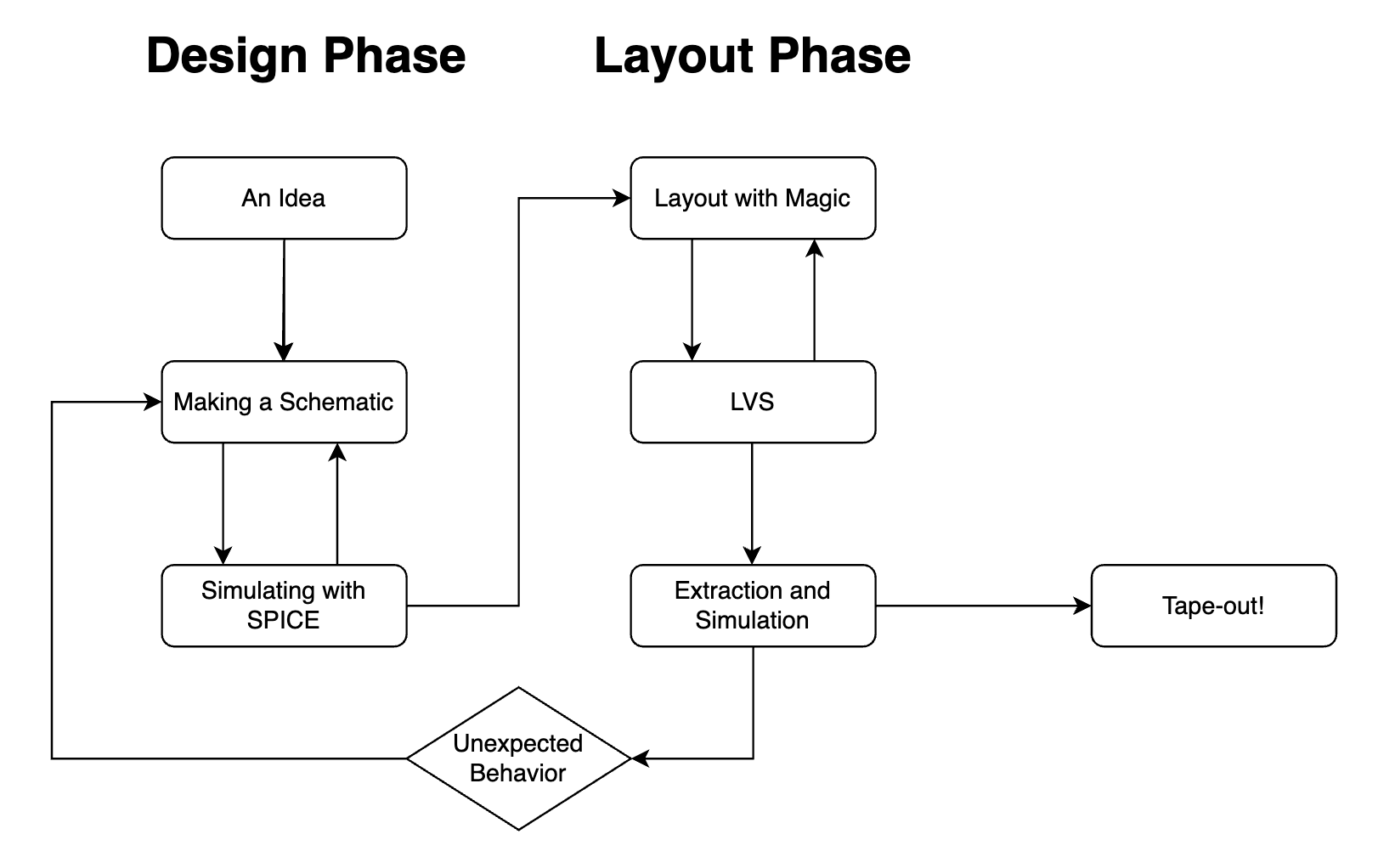
The Analog Subteam's Process Flow
To begin, we start with creating the circuit through XSCHEM.
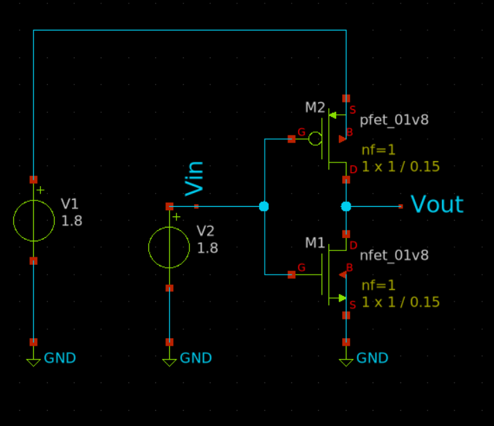
Schematic of the Inverter
After finalizing our schematic, we move on to testing with Ngspice, integrated into XSCHEM. We start by importing models from the SKY130 PDK to inform Ngspice about how our components should behave. Following this, we conduct specific tests to check the performance of our circuit. The choice of tests depends on the type of circuit we're working with. Typically, we perform transient analysis to observe how our design behaves over time. Subsequently, we proceed to frequency testing to assess the operational limits of our circuit. Ngspice provides a graphing tool to help us understand the circuit's response.
Below are some simulations:
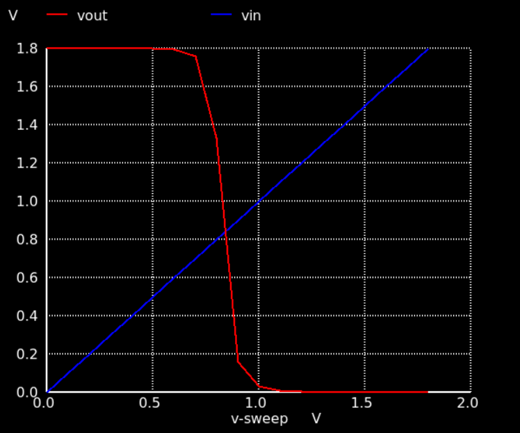
DC Voltage Stepping
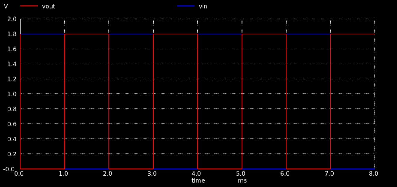
Transient of a Square Wave Input
Once our tests confirm the expected behavior, we transition to the layout phase.
Unlike digital design, analog circuits have to be laid out manually. This involves arranging our components and routing them with the materials available on the chip. The tool we use is called Magic VLSI. Before getting started, we must import the caravel magic files from Efabless. This will give us the chip's footprint so that we know where all the IO pads are. We can then import the devices used in our schematic into Magic and begin arranging them.

Layout of the Inverter in Magic
As we paint on the materials, we closely monitor that our layout is within the design requirements of SKY130. Some materials need sufficient spacing or have a minimum size requirement.
If our chip layout looks good and meets all the design specifications, we have to ensure that everything is connected properly.
To confirm the consistency between our Magic layout and the schematic designed in XSCHEM, we utilize Netgen software. This tool thoroughly examines the connections and devices within our Magic layout, comparing them with the schematic connections. This verification process is known as LVS, short for layout-versus-schematic. To get this to work, we have to export a complete description of the connections from both designs to a netlist. Netgen will process these netlists and give a rundown of how the circuits compare.
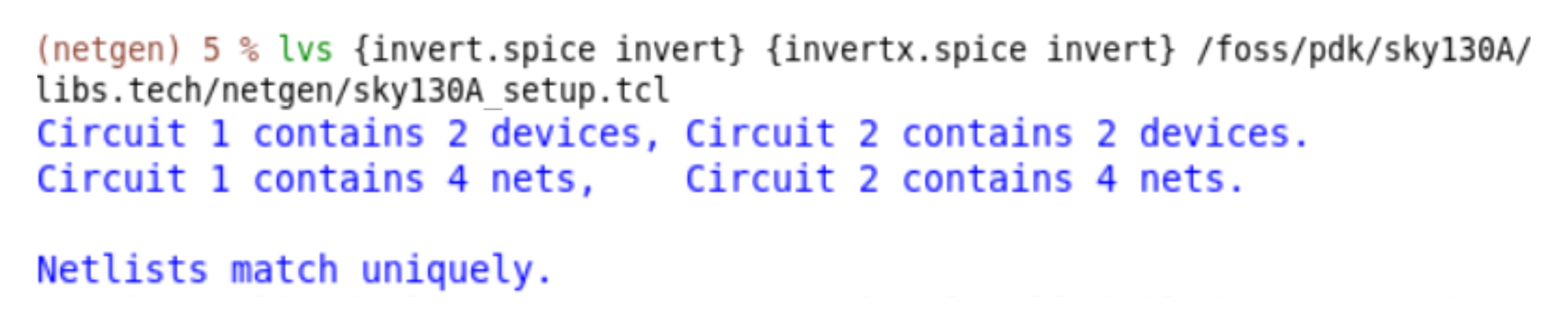
Netgen Output of LVS Test
If everything matches up, we can move on to the final step, simulating the extracted layout.
Unfortunately, the materials used in a chip are not ideal: they have some capacitance and resistivity, which we call "parasitics". However, we can model these approximate parasitic values from our Magic layout in a process called extraction. Instead of having idealized connections, the extracted netlist will have connections modeled by resistor and capacitor components. We can run the same simulations as before, but now with something that models how our design would act on a chip.
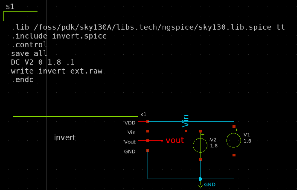
Extracted Circuit in XSCHEM

Extracted DC Sweep
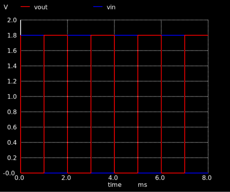
Extracted Transient
Seeing that our post-extraction simulations run as expected, we have completed the process flow!
Going from an idea to a chip can seem like an intimidating process, especially in the world of analog design. But, by writing this blog post, we hope we have broken down the process flow into small steps that are easier to follow and understand.