The SAR ADC: Refining Digital Output Bit by Bit
Anika Sukthankar
Dec 20, 2024
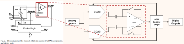
Hello! My name is Anika and I am on the project management subteam of C2S2. This semester, I expressed an interest in learning more about the analog subteam. More specifically, I learned extensively about the Successive Approximative Register Analog-to-Digital Converter, otherwise known as the SAR ADC. For reference, see Figure 1 below. A SAR ADC uses a binary search algorithm to approximate an input voltage.
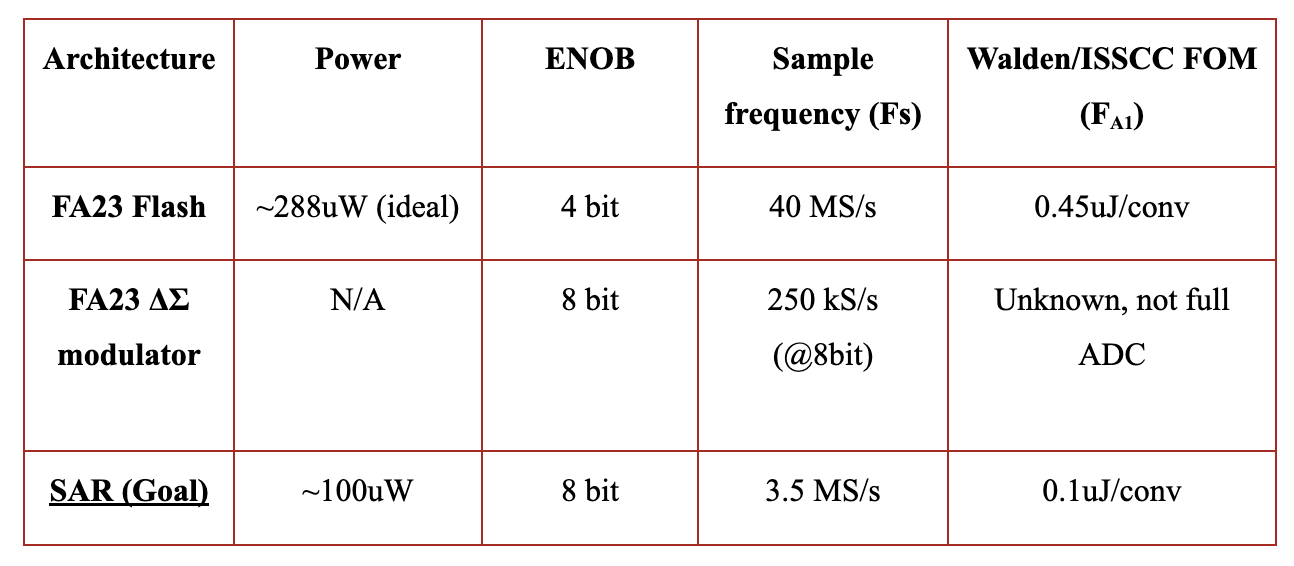
The team transitioned to a SAR ADC circuit for several reasons. First, they had several process and constraint requirements. These include a 130 nm CMOS process, meaning that this required low power and a low voltage process (1 v8). Another reason was that the area complexity scales were proportional to the number of bits. On the other hand, a Flash ADC requires more comparators, is more costly, and consumes more power, which is highly impractical for our circuit. Moreover, SAR ADCs are more common, and provide higher resolution despite a lower area and lower power. As shown in Figure 1, the Analog subteam constructed a chart comparing the SAR ADC to the Flash ADC and Modulator from previous year, as well as their goal for the SAR.
For more guidance on SAR ADC and its functions, I spoke with Daniel Kaminski ‘27 and Caden Xu ‘27 to learn more. Caden Xu likened the SAR ADC to a scale, saying:
“It’s like having a standard mass on one side and paper clips on the other. As you keep adding paper clips, it will eventually balance out. Same thing with SAR ADC. It takes your input voltage and then guesses a voltage, and then compares the two. If it guesses a voltage that is too high, it lowers that voltage. It continues approximating until it reaches the final value that the input voltage is.”
The SAR ADC has several components: a Capacitive DAC (CDAC), a comparator, and analog switches. First, the Successive Approximation Register (SAR) utilizes a binary search function and flip bits from the most significant bit (MSB) to the least significant bit (LSB). After each flip, it checks how the DAC voltage compares to the input voltage. It then changes the DAC input accordingly.
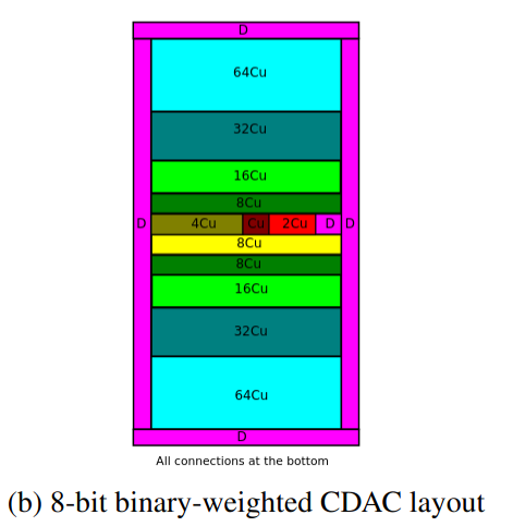
Next is the CDAC. Kaminiski tells us that the CDAC is used to convert a digital signal that is then provided into a voltage. The layout of the CDAC is shown in Figure 3 below. The CDAC has a binary, weighted 8 bit and differential configuration. This way, it reduces kickbacks (sudden, high spikes in voltage) and constraints on charge injection. The CDAC operates by switching capacitor connections. The layout of the CDAC is crucial for our circuit. First, the CDAC process variation and parasitics has a profound impact on the effective number of bits (ENOB). When designing the CDAC, the team had to keep their optimal layout for the overall SAR ADC in mind, as the CDAC had to be thoroughly tested before the layout was designed.
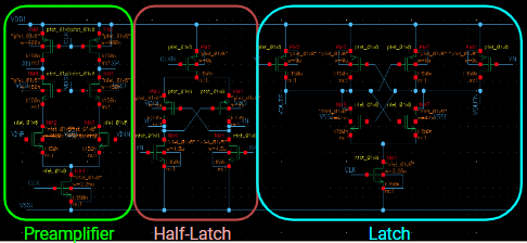
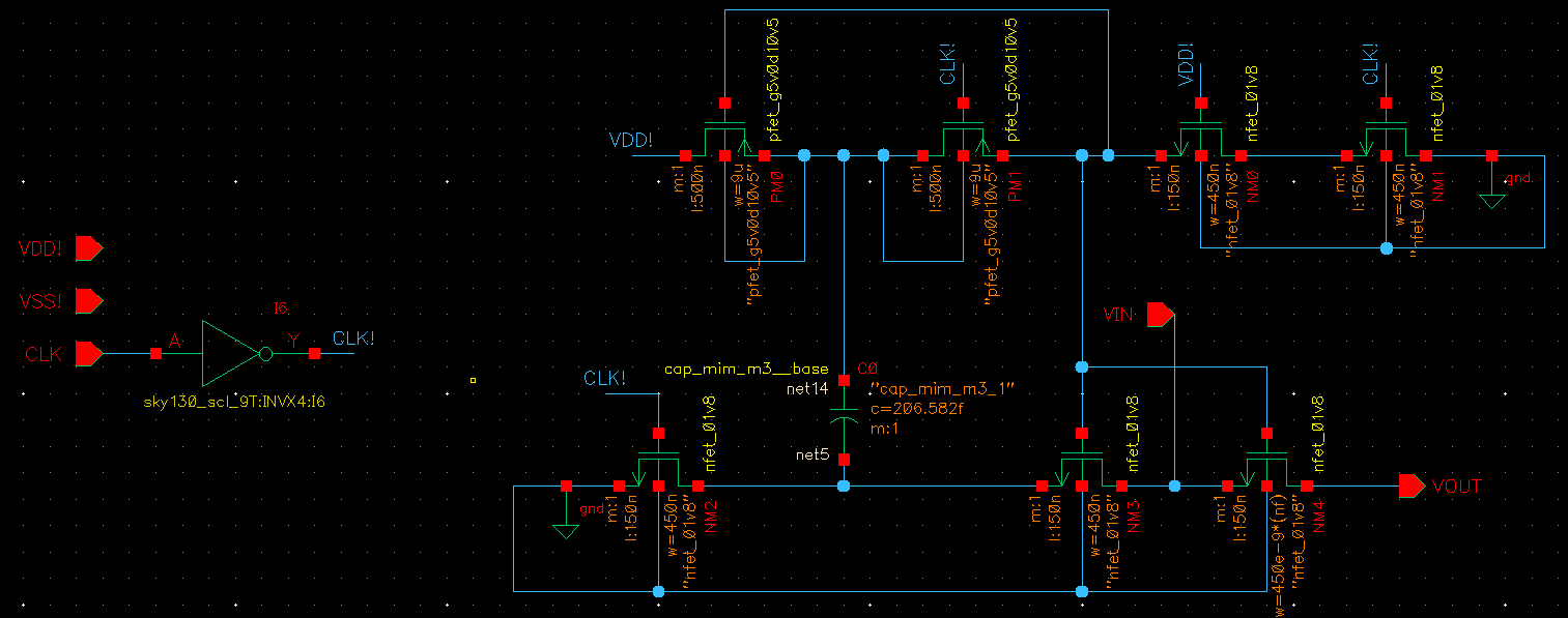
Another component is the comparator, which compares 2 signals together. It was designed so that it is both accurate and has a resolution. The Analog subteam designed a Triple Tail Latched comparator, as shown in the Figure 4 below. The Triple Comparator has several advantages, as it is a high speed application, generates little to no noise, and performs well with low power consumption. It consists of three stages: the preamplifier, the half-latch, and the latch. The preamplifier is responsible for amplifying the differences between input signals, which allows the other stages to detect differences in voltage. Next, the half-latch stage is the core of the comparator. It utilizes a differential amplifier circuit with transistors to amplify the voltage difference given by the preamplifier stage. Last is the latch stage, which provides a binary output based on the given voltage difference from the half-latch stage.
The last component is the analog switch, which switches the analog voltage to the capacitors. As shown in Figure 5, the Analog team decided to implement a bootstrapped analog switch. This allows for a selective switching between different analog signals. Furthermore, this design maintains a constant Vgs and a constant-on resistance, thus minimizing any distortion caused by the switch’s resistance changing with the input signal. Xu states that this lack of distortion is what makes it perfect for ADCs, where he says “precision is key."
After all of their hard work this semester, the Analog subteam has successfully implemented a function 4 bit SAR ADC, which has a latched output and easier digital interfacing. In addition, the high AMS simulation speed allows it to quickly iterate. This allows for a function simulation with Verilog and synthesized logic when testing for transistor levels. Moreover, the Analog team says that it is now possible to co-simulate this with the Digital Subteam, meaning that the full chip can now be tested.
Overall, the Analog subteam has showcased incredible growth and a steep learning curve. Simple research of an interesting topic and the motivation to improve from previous designs has developed into a remarkable final product. The SAR ADC is proof of the Analog subteam’s dedication and passion for chip design, as they shape the future of chip design, one bit at a time.