Building from the Ground Up: The Platforms Subteam's Evolution
Adele Thompson
Dec 19, 2024
At the beginning of the semester, the Platforms subteam started with a single goal: designing a PCB to support the digital team's tapeout. The first critical step was figuring out how to power this PCB. After thoroughly researching various power options, they identified two key requirements: the PCB needed to work both with USB power and independently, making a rechargeable battery the ideal solution.
The team then went through a careful selection process for their power source, considering several requirements. They needed something small enough to fit their limited PCB space, but powerful enough to run all their components. The 3.7V, 200mAh coin cell battery was a well-suited solution. It is small which worked perfectly within their space constraints, while its 200mAh capacity packed enough power to run everything from IMUs to microphones for long periods. The battery's 3.7V output was another key aspect. It aligned perfectly with their circuit's voltage requirements, eliminating the need for complex voltage conversion systems that would have taken up more board space and added unnecessary complexity.
Selecting the battery was just the start. Next came the task of designing the charging circuit. The team simulated different charging solutions in LTSpice, comparing their efficiency and performance. After extensive testing, they selected the MCP73834-NVIUN charger. Their simulations showed impressive results. It could fully charge the battery in under three seconds while maintaining thermal safety and optimal energy usage. This charger also included built-in thermal regulation, making it efficient and safe.
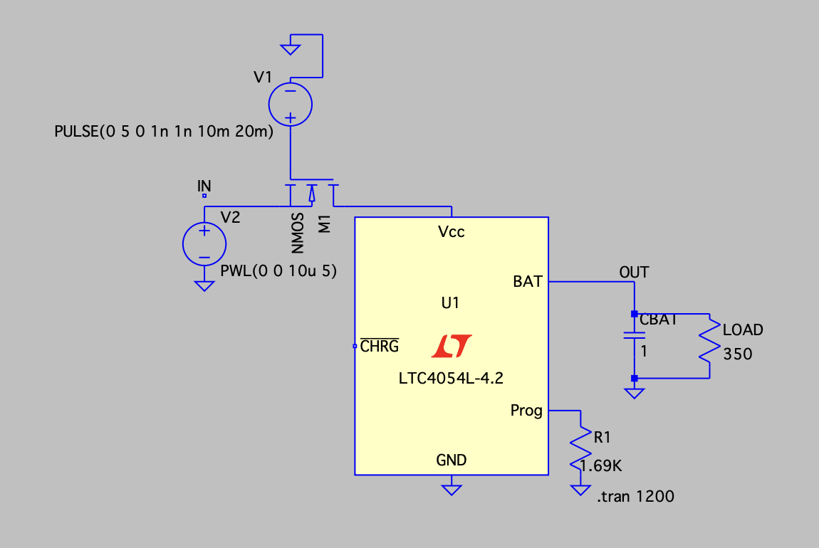
MCP73834-NVIUN charger
The team developed an agnostic PCB - essentially a digital board designed to support testing needs. They designed it with a 4-layer stack: a top signal layer for components and routing, a power plane, a ground plane, and a bottom signal layer for additional routing paths. This layer configuration was crucial for maintaining signal integrity by providing consistent power delivery and minimizing noise between signals.
While the team initially began exploring mixed-signal PCB development, this project was temporarily halted. Instead, they redirected their focus to developing a specialized analog board, with particular attention to microphone input integration. This analog PCB, being designed in KiCad, represents their expansion into new technical territories.
Collaboration has been significant to the platform subteam's success. They work closely with the other subteams to understand exactly what components each group needs. Through this journey, the team has developed more knowledge in PCB design, from flash memory to microphones and IMUs, ensuring each component's specifications align perfectly with the Carvel harness and pinout configurations.
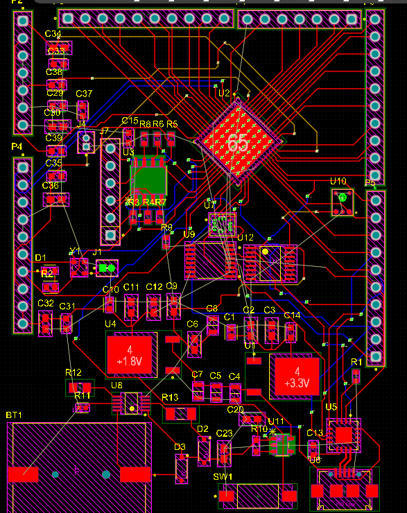
Agnostic Board Routing
The team has been making steady progress on multiple fronts. After completing their Design Rule Check (DRC), the agnostic board is now in fabrication and will soon be ready for testing digital chip designs. Meanwhile, development continues on the analog PCB, which is scheduled for fabrication next semester. New team members are gaining valuable experience by working on the STM32 PCB design in KiCad, building skills that will prove valuable as they continue their PCB design journey.
The Platforms subteam's journey showcases how engineering projects evolve from initial component selection through complex system integration. What started as a focused effort to support digital tape-outs has grown into a comprehensive platform development effort. Their work sets a foundation to support future projects across multiple domains, demonstrating their commitment to advancing custom silicon systems.