Unboxing C2S2's 2024 Spring Tape Outs!
Jason Wang
Dec 8, 2024
C2S2 is a Cornell Engineering Project Team focused on advancing undergraduate custom semiconductor design. Collaborating with the Lab of Ornithology and contributing to the open-source silicon ecosystem, we utilize Efabless and Sky130 for digital, analog, and mixed-signal chip development. Over the past two years, we have designed and taped out chips twice annually. Recently, we received our Spring 2024 Digital and Spring 2024 Analog tape-outs. While the team finalizes the chip names, let's explore their designs, physical tape-outs, and ongoing testing!
The Digital Chip - Design
The Spring 2024 tape-out is a modular digital chip packed with features for flexible signal processing. It includes a 16-bit fixed-point 32-point FFT module to analyze signals in the frequency domain and a configurable classifier to filter and classify audio signals based on frequency, amplitude, and sampling rate. The design incorporates three dynamic crossbars that enable flexible data routing between modules or external interfaces, such as SPI, Wishbone, and GPIOs. Messages sent to the chip are 20 bits wide, with the top 4 bits used for addressing and the bottom 16 for data or configuration. A modified SPI testing framework streamlines the testing process by automating data flow simulations and validating the chip's functionality, making it adaptable to diverse signal processing and system integration tasks.
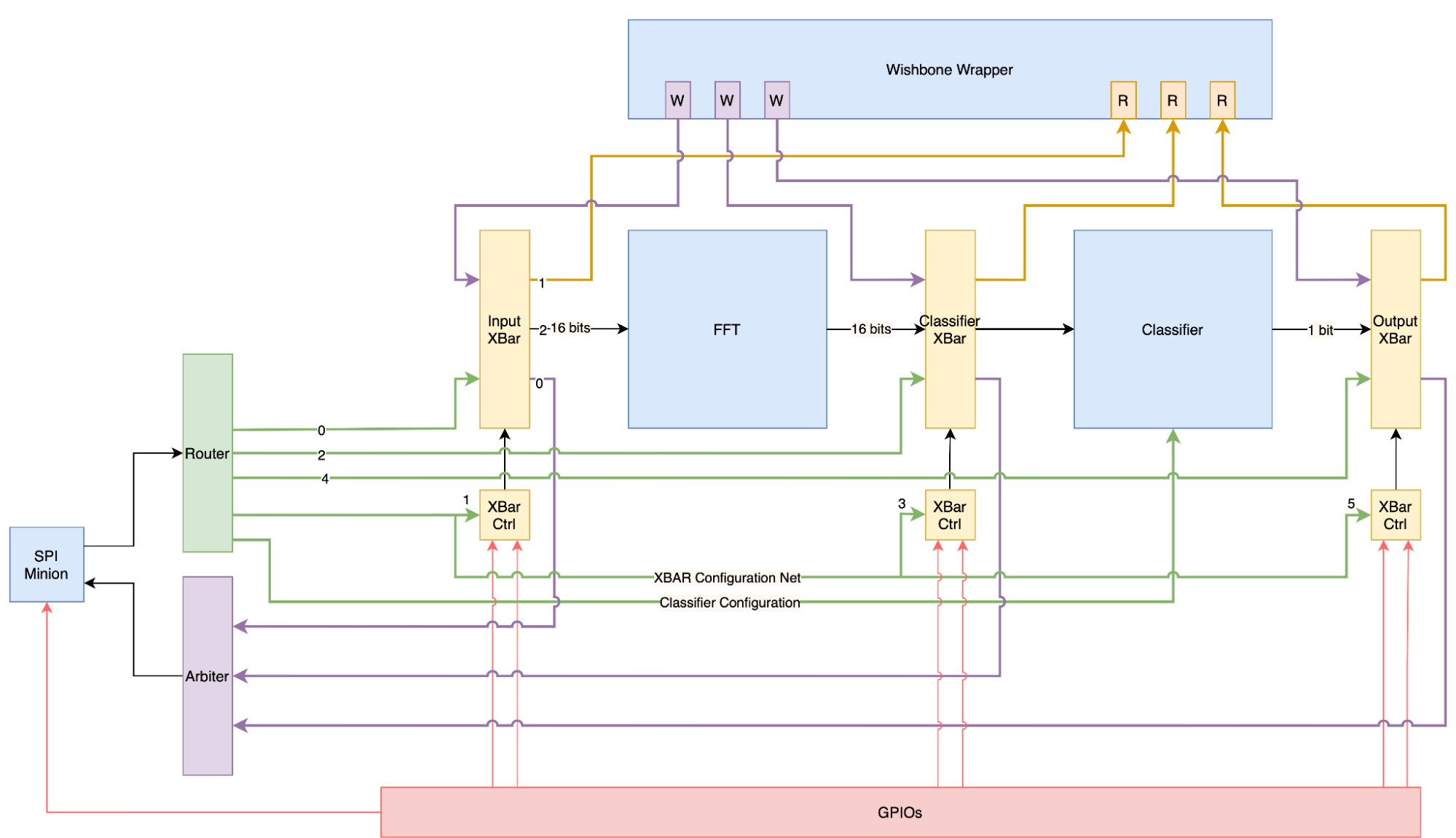
The Block Diagram of the Spring 2024 Digital Chip
The Analog Chip - Design
The Spring 2024 Analog Chip is designed to bridge continuous analog signals with digital systems using two specialized Analog-to-Digital Converters (ADCs). The Delta-Sigma Modulator prioritizes high resolution and noise-shaping capabilities, making it ideal for precise, low-frequency signal processing, such as audio and environmental data. The Flash ADC, on the other hand, excels in rapid signal conversion, enabling high-speed applications like real-time monitoring. Together, these ADCs provide a versatile platform capable of handling both accuracy-demanding and high-throughput scenarios.

Rendering Photos of the Spring 2024 Analog Chip
Tape-out
A tape-out is the final stage of chip design where the completed schematics are sent for fabrication, producing physical silicon chips. In the box, we received both bare dies, raw silicon chips, and packaged versions, where the dies are encased for protection and connectivity. These tapeouts mark the transition from design to hardware, paving the way for real-world testing.
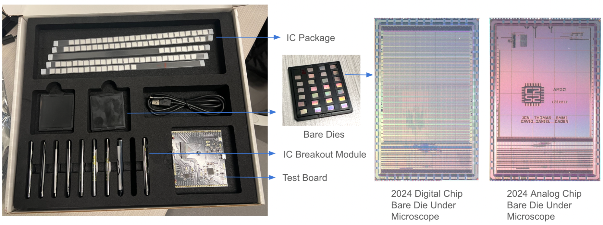
Unboxing the Efabless package - Bare Dies, Prototyping Module, and the Test Board
Digital and Analog Chips Testing
Both the Digital and Analog chips are undergoing rigorous testing to validate their performance and functionality. For the Digital Chip, automated pytest scripts have verified the interconnect functionality and data routing, confirming that paths such as classifier input/output and loopback configurations are operating as designed. All tests have been successfully passed, demonstrating that the chip is fully functional and ready for integration into further systems.
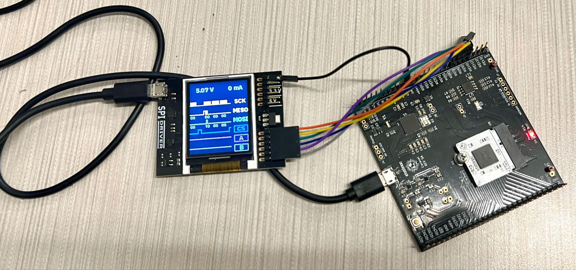
Digital Chip Testing Setup
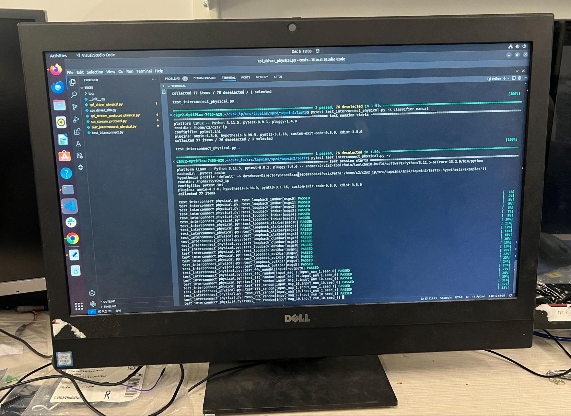
Digital Chip Tests Ongoing and Running at the ELL C2 Computer
For the Analog Chip, testing emphasizes the performance of the ADCs in real-world conditions, which have manufacturing imperfections and variations. Signal plots and oscilloscope traces reveal detailed behavior, providing insight into the Delta-Sigma Modulator and Flash ADC performance. The oscilloscope trace represents the output of the Flash ADC, and the sliding window plot allows the analog team to estimate the Delta Sigma ADC performance.
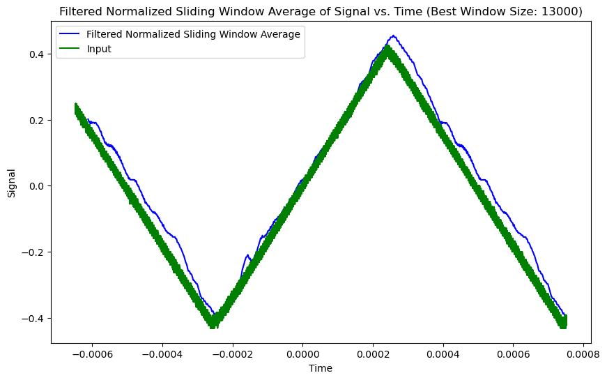
Delta Sigma Modulator Tested and Worked in Preliminary Testing
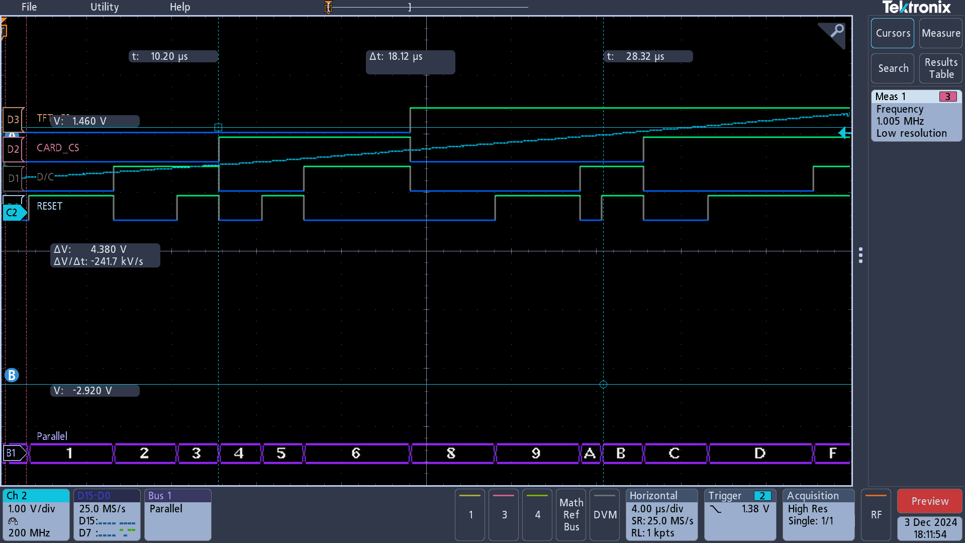
Flash ADC Tested and Worked in Preliminary Testing
Both chips leverage a shared modular testing setup, where packaged devices are mounted on white Efabless PCBs connected to black testing PCBs. This framework supplies power, clock signals, and SPI interfaces, enabling seamless integration of digital and analog signals for comprehensive validation. With ongoing tests, the team is gaining valuable insights to refine these designs further-stay tuned for more updates as our work continues!
