Analog Multiplexer
Adele Thompson and David Bertuch
April 2nd, 2023
Hello everyone! As new members of C2S2, we were tasked with building an analog multiplexer using digital logic gates and MOSFETs. Since we are limited by the number of output pins on a chip, a MUX would allow us to measure more signals on the circuit.
Our idea for the analog MUX is fundamentally different from a digital MUX. In the digital case, you would typically see the input signal combined with the select logic.

2-to-1 Digital Multiplexer
You can see that an analog signal would not be compatible with this design. Because of this, we decided to break our multiplexer into two parts: a decoder and an analog switch array.
To start, we designed a decoder (Figure 2) using NAND and NOT gates. Each output (and its inverse) is connected to an analog switch (Figure 3). The decoder uses a 4-bit digital input to select one of the 16 possible analog switches. This selection turns on a MOSFET pass-gate that connects the desired signal to the analog output.
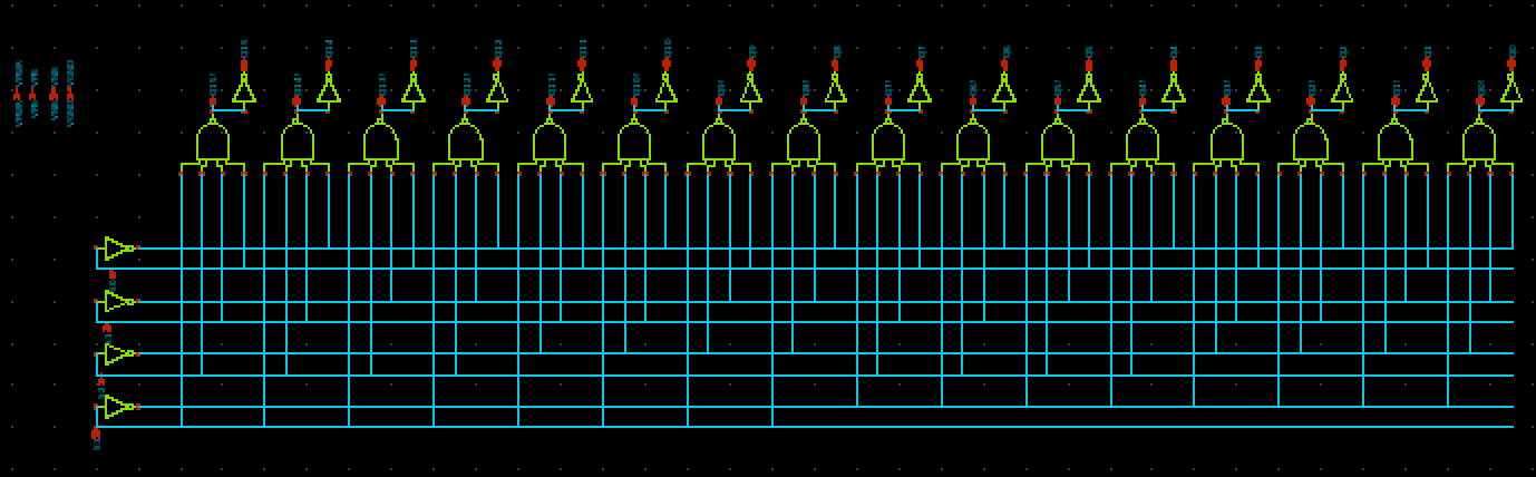
4-to-16 Digital Decoder
The second part of our circuit is made up of 16 analog switches. These switches are MOSFET pass-gates made from complementary transistor pairs (Figure 3). Each analog signal enters the switch's source, and the switches' drains are tied together to form the MUX output (see Figure 4). Each switch was designed to have low on-resistance to ensure minimal signal loss and maximum signal quality. It is also essential to ensure the on-resistance is linear across the range of voltages we use. The MOSFET switches are controlled by the digital decoder and can be turned on or off depending on the selected input.
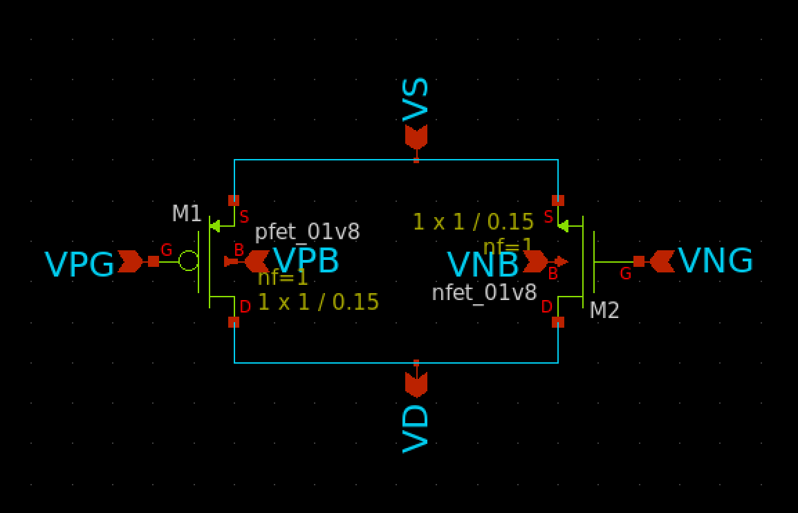
Analog switch made from a complementary MOSFET pair (VPG and VNG must take opposite signals)
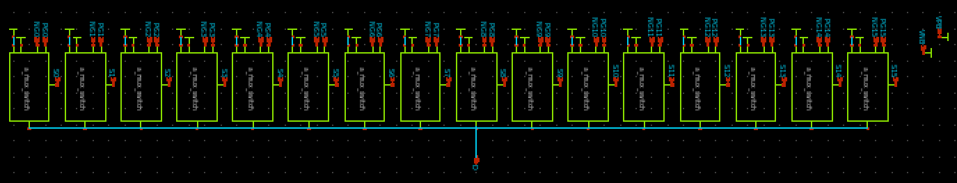
16 Analog Switches (modeled as boxes) with Connected Drains
After we had completed the design and construction of the analog mux, we tested it using all 16 truth table values. We were pleased to find that it works as expected.
To optimize the performance of the MUX, we went back to test the on-resistance of an individual switch (Figure 3). We are currently working on this to minimize the loss of input signals and to linearize the resistance. This is a matter of adjusting the MOSFET aspect ratios.
One of the key benefits of an analog mux is that it can take in both analog and digital inputs, making it incredibly versatile for circuit design. Our project aimed to create more outputs for an analog circuit design, and with the successful creation of our analog mux, we were able to achieve just that.
Overall, the project was a challenging but rewarding experience for us. We were able to put our skills in digital logic gates and MOSFET transistors to practical use and create a functional and useful analog mux. We are excited to continue exploring and expanding our knowledge and look forward to future projects and challenges.

Analog Mux from the Decoder and 16 signal Analog Switch
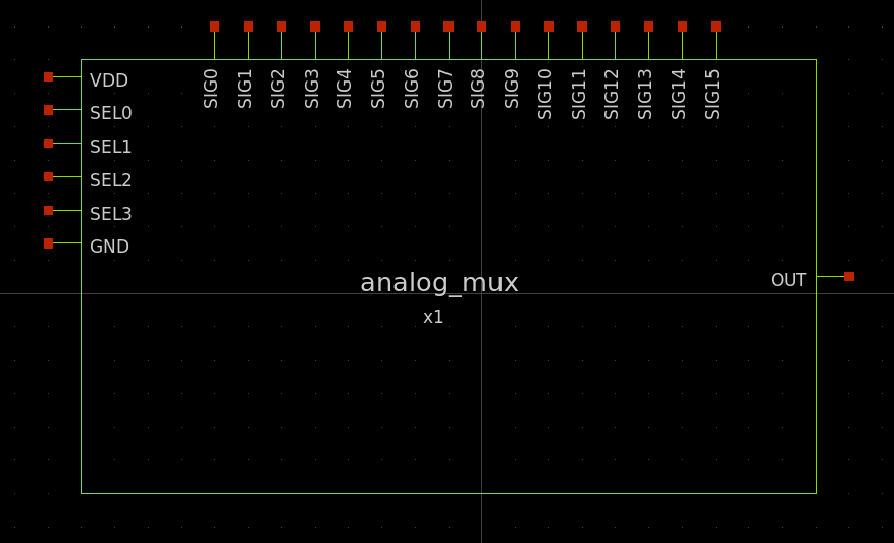
Top-level Symbol of the Analog MUX