Constant-gm Current Reference Tape-In
Jon Ho and Emmi Wyttenbach
March 12th, 2023
To set the stage for this blog post, we believe it is worth discussing C2S2's overall mission: providing undergraduates with the opportunity to tape-out both analog and digital integrated circuits by leveraging open-source EDA tools and importantly, the open-source Skywater 130nm PDK. Emmi and I are members of C2S2's analog sub-team. Our goal within C2S2's overarching mission is to tape-out a two-stage operational amplifier (OTA) with an on-chip current reference this June (via Efabless' 2306 chipIgnite shuttle). Though our two-stage OTA does not - by any stretch of the imagination - qualify as a novel or groundbreaking circuit, we believe it will serve as a stepping stone for future undergraduate chip designers at Cornell University. It is important to note that as a sub-team, our battle not only lies with circuit design, but also with the open-source analog EDA tools that can be a challenge to use. No other team at Cornell University has taped-out an analog chip using Sky130.
As mentioned earlier, our tapeout is centered around a two-stage OTA with an on-chip current reference (Figure 1). For this tape-in we decided to lay out the on-chip current reference, which is simply a constant-gm current source as pictured in Figure 2. At a high-level, the constant-gm current source utilizes negative feedback to maintain a constant current: the NMOS current mirror in the left branch mirrors current over to the right branch, which then mirrors current back to the left branch by means of the PMOS current mirror. Importantly, it can be shown that the current provided by a constant-gm source depends on the resistor in the right branch, and the aspect ratio of the transistors (as well as some other process parameters). However, the current provided by this circuit is not a function of VDD, which is a desirable trait (this is known as supply independent biasing). We designed all of our circuits, including this constant-gm current source, around a VDD of 1.8V. Furthermore, we designed this constant-gm current source to provide 17uA of current. This 17uA of current is then mirrored (and multiplied in the process) to the tail current transistor of the OTA, which is designed to draw 250uA of current.
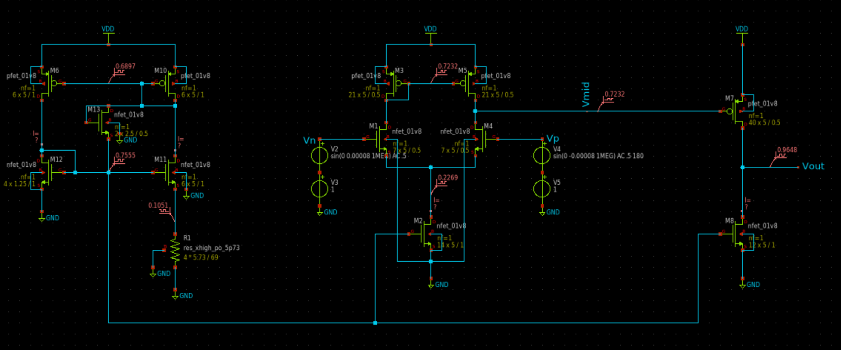
Schematic for Two-stage OTA with On-Chip Current Reference
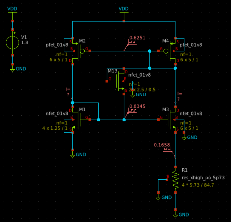
Schematic for Constant-gm Current Source
Continuing with our brief analysis of the constant-gm current reference, it is also worth noting that all of the transistors are 1um long. These (relatively) long-channel devices are less sensitive to channel-length modulation, a phenomenon resulting in the drain current of a transistor being dependent on VDS. This can throw off the amount of current provided by the transistors if the VDS of any particular device is abnormally high, since current mirroring relies on the fact that drain current is mainly a function of VGS. The transistors also utilize an even-numbered multiplier for better symmetry during layout.
Let us now turn our attention to the transistor in the center of the constant-gm circuit (transistor M13 in Figure 2). This transistor's purpose is to ensure proper start-up functionality. A constant-gm circuit can exist in one of two stable states: it can either supply the desired current, or it can supply no current at all (i.e., all devices are in cutoff). To prevent the latter condition from occurring, we place a diode-connected transistor between the two diode-connected transistors in the left and right branches. This way, there is a (small) current path between VDD and ground during startup; this small current allows the other devices in the circuit to turn on by charging their gate capacitances. We also note that the voltage we are mirroring is the voltage seen at the gate of the NMOS current-mirror. By adjusting the aspect ratio of the device that is mirroring our constant-gm's voltage, the current can either be multiplied or divided. Finally, we observe that the resistor on the right branch contains 4 segments that are each 5.73um wide and 69um long. Initially, we had a sub-micron-long resistor that provided us the correct resistance value during simulation. However, we soon realized that a resistor with such small physical dimensions would be sensitive to any size variations during the fabrication process. With this in mind, we scaled up the size of the resistor significantly and utilized multipliers for matching-purposes during layout.
To evaluate the reliability and robustness of our constant-gm current reference, we performed several different simulations. First, we performed DC simulations using Ngspice and swept the supply voltage between 1.6V and 2.2V. Since the current provided by this circuit is supposed to be supply-independent by design, we expect a small variation in supplied current. Indeed, this is the case: the current only varies by 1uA across a 0.6V sweep over VDD. Similarly, the NMOS gate voltage in the circuit varies by very little over the same sweep; this is to be expected since this is the gate voltage that is used to mirror current.
Next, we simulated start-up conditions using transient analysis. By setting the node voltages of the circuit to be 0V initially (via the initial condition spice directives) and by setting VDD to 1.8V, we can test to see if the circuit truly settles to its desired state condition. As can be seen in Figure 3, the node voltages within the circuit start at 0 and eventually rise to their appropriate voltages. This is a direct consequence of the current through the transistor M13, which starts at XX uA and dies down to 0A during steady-state operation. It is important to note that under steady-state conditions, the start-up transistor is not on; this is clearly shown by the bias-voltages associated with this transistor.
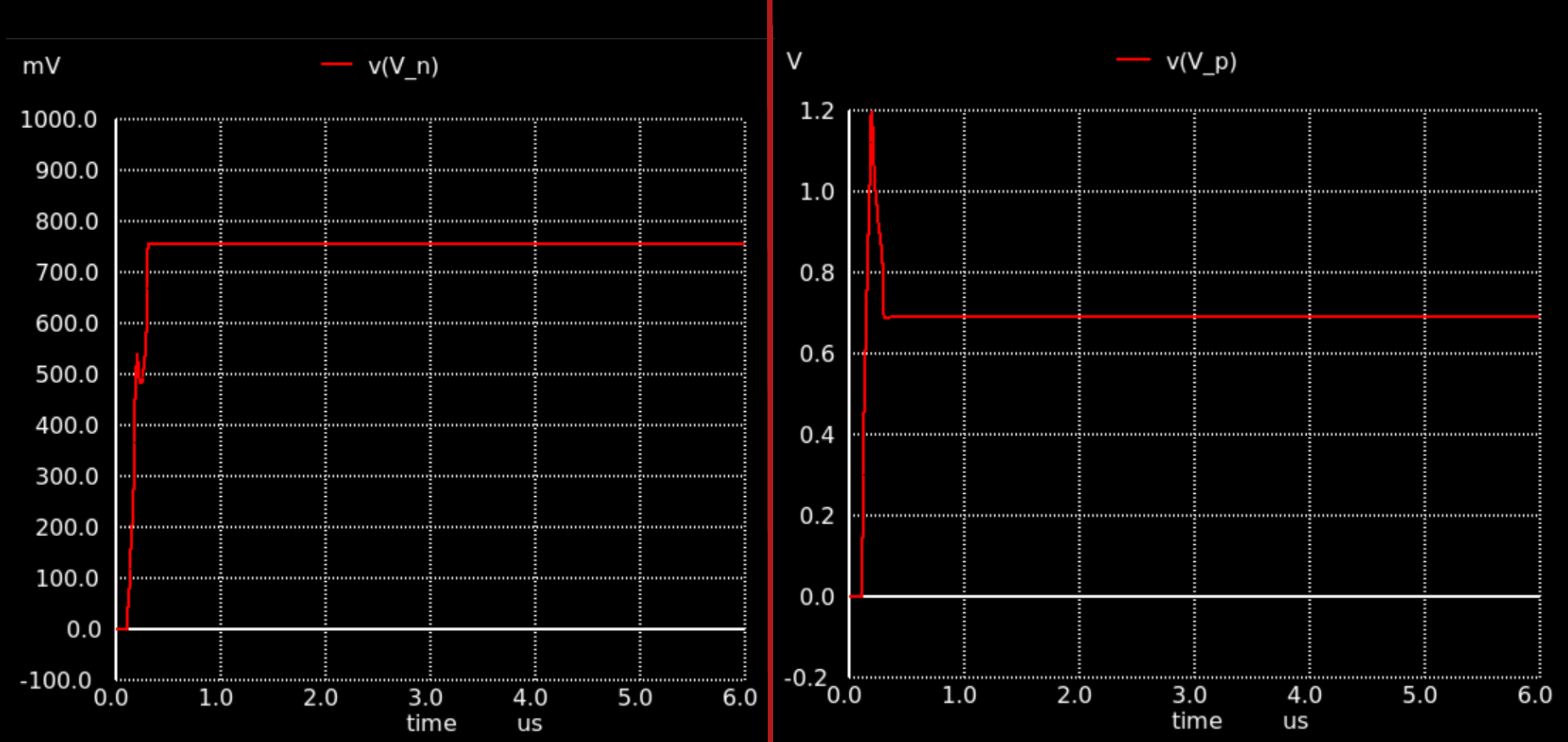
NMOS Gate Voltage Over Time (left), PMOS Gate Voltage Over Time (right)
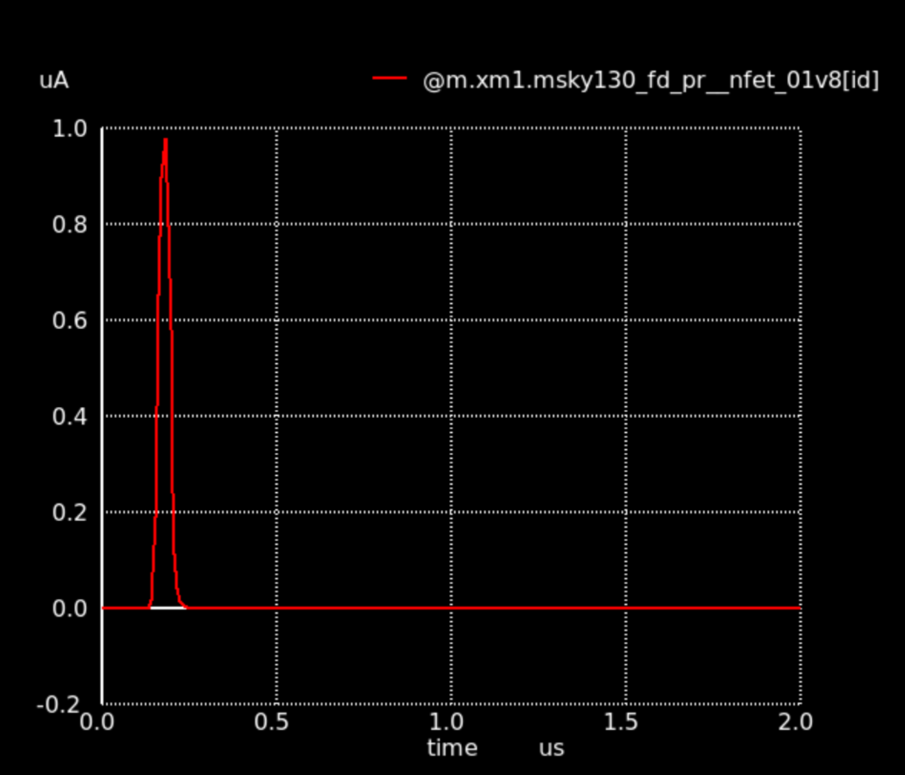
Current Through M13 Over Time
After performing the aforementioned simulations, we proceeded to lay out our circuit using Magic. During our floor-planning, we decided to use a y-axis of symmetry to guide our layout. By using this axis of symmetry, each device should be similarly affected by process variation. Under this layout philosophy, the transistors are placed in horizontal rows; transistors are then stacked vertically. As a team, we decided to use M1 to make horizontal connections; M2 to make vertical connections; and so forth. A completed layout is shown in Figure 5.
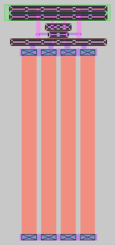
Constant-gm Layout
Next, we instanted our layout of the constant-gm source within Efabless' Caravan pad-ring. We then routed traces from the pads to our design. Importantly, we used two pads for power and ground, and two pads to probe the voltage at the gate of the NMOS current mirror and the current at the bottom of the resistor. After completing the integration of our design into the provided padring, we performed DRC and LVS checks. LVS was performed by Netgen, which compares the spice netlist generated by the schematic capture tool Xschem and the spice netlist generated by Magic. After ensuring that our design was DRC and LVS clean, we then used Magic to perform a full parasitic extraction. The extracted spice file was tied to a schematic symbol of the constant-gm circuit so we could perform the same pre-layout simulations. Unfortunately, all of the currents and voltages were nonsensical in terms of their values; none of the values made any physical sense. After many hours of debugging, and after speaking with Tim Edwards, we realized that Efabless' provided schematic symbol does not correctly perform port-ordering. In other words, the ports on our layout do not match the ports in our schematic. This mismatch resulted in us viewing the values at ports that we did not wish to probe during post-extraction simulation. After working with Tim Edwards, he kindly helped us resolve this issue by providing us with the correct schematic symbol. Furthermore, this fix was pushed to the Github page for analog Caravan projects.
Returning back to post-extraction simulation, we can view the results in Figure 6. These results are in the correct order of magnitude (as compared to ideal simulation results) and match our intuition for how a constant-gm current source should behave. Unfortunately, the current provided by the circuit was approximately 3uA, as opposed to the desired 17uA. We realized this discrepancy was due to the fact that the traces between the constant-gm circuit and the pads (in layout) were a few millimeters in length, resulting in a massive IR drop. Armed with this knowledge, we performed full parasitic extraction of just the constant-gm circuit without the pad-ring and then performed the post-extraction simulations. As shown in Figure 7, the performance of the extracted constant-gm circuit (without the IR drops associated with global routing) and the ideal constant-gm circuit are nearly identical.
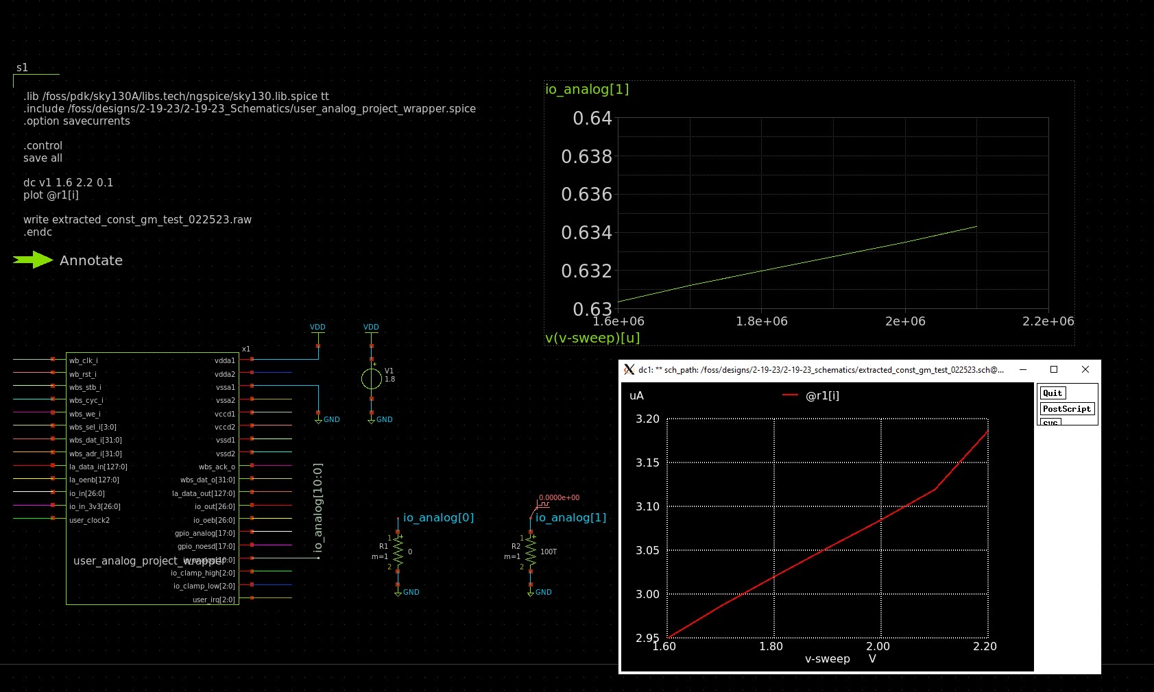
Post-Extraction Simulation Results of Constant-gm Circuit Connected to the Pad Ring

Constant-gm Current as a Function of Supply Voltage (left), NMOS Gate Voltage as a Function of Supply Voltage (right)
Ultimately, this tape-in was an invaluable experience. First, it provided us the opportunity to learn how to use the open-source tools associated with the Sky130 analog design flow. Second, we learned how to layout devices and perform DRC and LVS checks. Third, we learned how to perform parasitic extraction, and post-extraction simulations. Lastly, this tape-in provides our sub-team with confidence. We now have a constant-gm circuit that has been laid-out, extracted, and tested with parasitics. Furthermore, this design passes all of Efabless' online pre-checks and is tape-out ready. Armed with this tape-in experience, our layout of the amplifier itself should be smoother and quicker. In general, this tape-in provided our team with a greater feeling of confidence; we firmly believe that we can make the tapeout deadline in June.