Deserializer and Tape-Out Update
Vicky Le
May 7th, 2023
Welcome to the final set of blog posts for the 2022 to 2023 academic year! My name is Vicky Le, and I am currently a sophomore studying Electrical and Computer Engineering and I am a member of the digital subteam working on the FFT(Fast Fourier Transform) project. Since my start on this team in August, I have been able to watch and contribute to C2S2's growth from a team of less than 10 to a team of over 30 members across several subteams and coming from a variety of backgrounds. Additionally, I have seen our progression throughout the year from starting with having rough ideas where to get started and what to do, to having a work process and now a full design which is ready for tape-out and sent for fabrication. It has truly been an amazing experience working with everyone, and being able to participate in a team that is working creatively and cooperatively in order to pave the way for others to also be able to leverage the open-source tools available to create chips.
Over the course of the year I worked on learning more about digital design by creating a deserializer, learning more about chip design and getting familiar with the open-source tools available, and learning about the verification process. Throughout this learning process I have used multiple tools and skills including coding in Verilog for block design, using PyMTL in order to create test benches, and pushing designs through OpenLane and OpenROAD in order to characterize the block such as obtaining information regarding the area or energy consumption. All of these tools and coding languages are easily accessible and can be used in order to create your own digital designs. Now I will walk you through how I worked with my team to create the deserializer using the tools and skills listed above.
For the FFT the deserializer is a block before the FFT that takes a long message and splits it up into multiple registers so that the FFT can use these chunks for computation. Figure 1 shows a high level block diagram and the components of the deserializer. The 4 signals at the top are the val-rdy interface which tells the deserializer and blocks connected to it whether it is ready to receive or send data in addition to whether the data leaving and entering the block is valid. Additionally the deserializer takes a message and clock signal as input and outputs an array of messages.
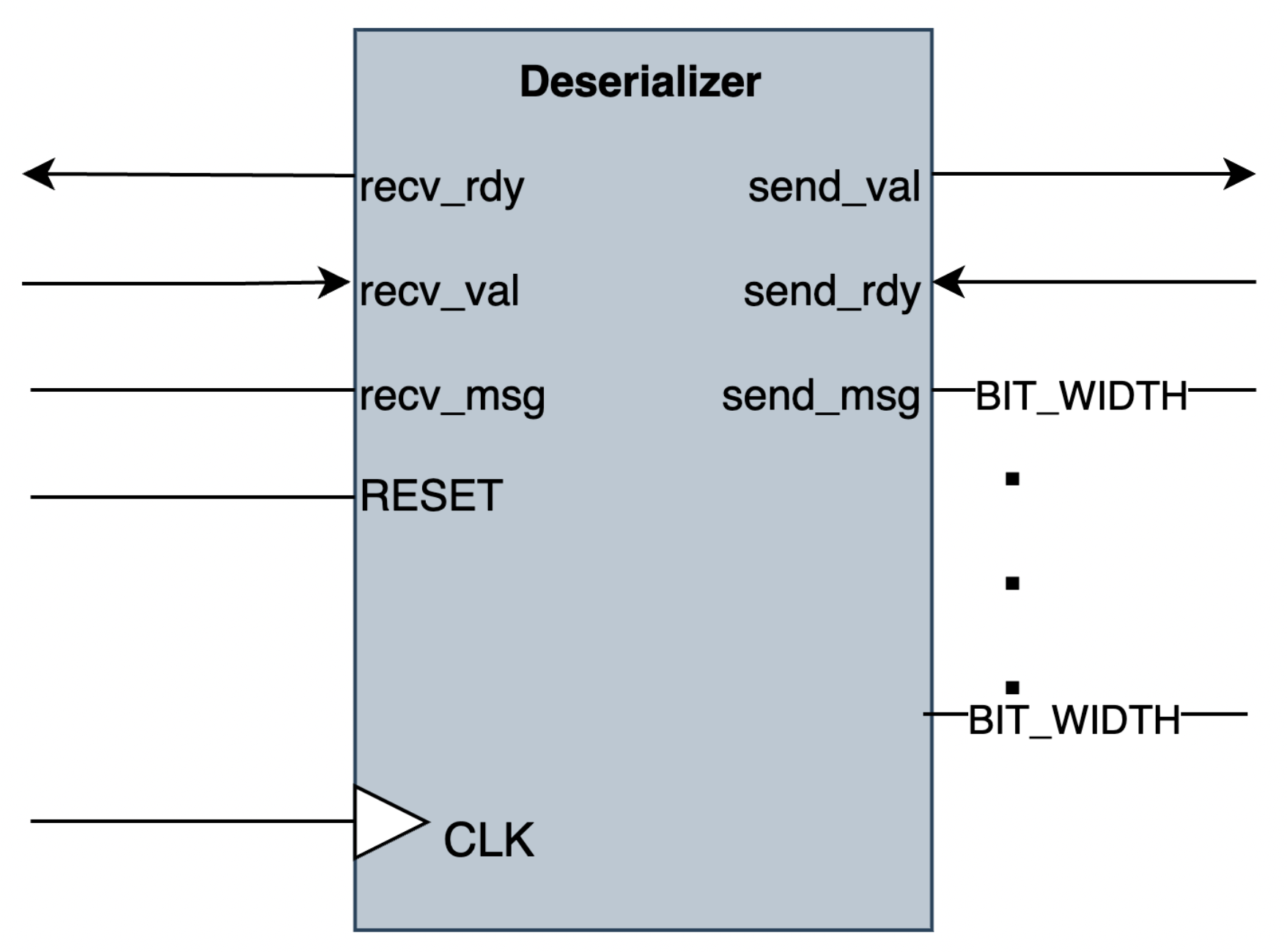
Block Diagram of the Deserializer
To design the deserializer the multiple smaller blocks were created and taken from the C2S2 module library. These blocks include a resettable register, decoder, and a control block. The control block takes the form of a finite state machine meaning that based on the input into the block a certain state will be entered and the output will be changed according to the state. In particular the control block determines the count which is then sent to a decoder which is one-bit hot so that it can enable a single register at a time to write data to. The decoder takes an input of the count from the control block and depending on the input will shift a 1 a certain number of bits. In the top module of the deserializer an instance of the control block and decoder is created and a generate block to create multiple registers is done, so that the control block increments count which is then sent to the decoder to enable a register to write data to. This process of writing to the registers continues until all registers are written to, and at this point the output is valid and the send_val and send_rdy will be set to 1. Figure 2 shows a more detailed block diagram of the deserializer and its individual components.
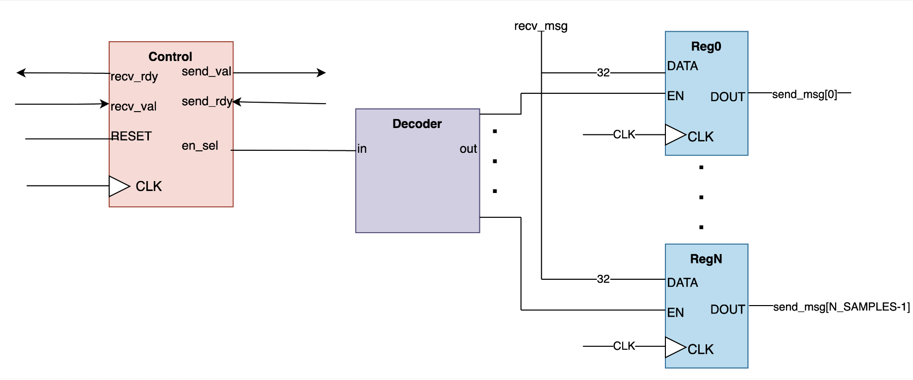
Deserializer Components and Connections
Now that the design portion of the deserializer is complete, the verification portion can begin. Verification for all blocks is essential to check that designs are functioning according to our design goals. To begin verification a test harness is created, so testing does not have to be done cycle by cycle. This test harness contains an instance of the deserializer module and a for loop such that it will set bits of the output message. In addition to the test harness file a python file is created in order to write the test cases and compare the inputs and outputs of the block to ensure the deserializer is functioning correctly. Figure 3 shows an example test case. Using these 2 files multiple test cases were created to ensure the block was functioning correctly. With these steps the deserializer was created for the FFT input.
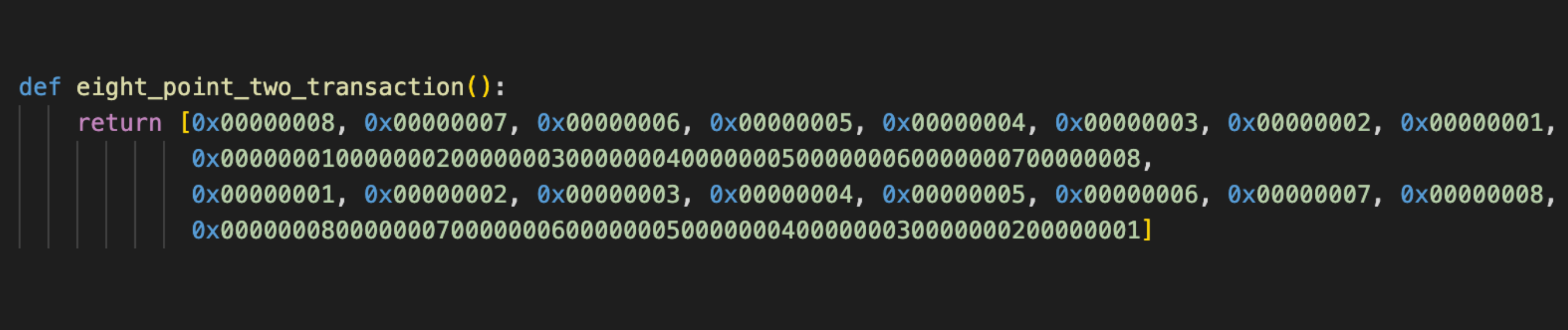
Example Test Case for Deserializer
Overall this year has been an incredible experience and we have been able to accomplish many big milestones including 2 tape-ins and soon our first tape-out as a digital subteam. Although it has been a challenging journey, we have been able to do great work and we are excited to continue. We can't wait to come back in the fall, so stay tuned to see our work next year! Thank you for reading our blog post and for keeping up with C2S2!