I SPI
Austin Brown and Mika Finkman
April 2nd, 2023
Hello! My name is Austin Brown. I am on the digital subteam for C2S2. I am a senior studying Information Science. Though my major does not typically interact with hardware, I found an interest in digital IC design through the computer architecture class I took during my junior year. I have enjoyed the opportunity to create components for ASICs and learning the different design details that go into them.
One of our goals this semester is to support the communication between the microphone and the rest of our chip. To do this, we are using the Serial Peripheral Interface, or SPI, communication protocol to communicate with the microphone.
There are two sides needed for SPI. Our naming convention for the two parts are the master and minion side. The master component is on the side of the system that drives the communication to the peripheral device. In this case, it will be our taped-out chip. The minion side would generally be the peripheral device that the main system is polling from. In this case, it is the microphone.
We were able to have a working SPI unit from last semester. However, there were limitations to the design. First, only SPI mode 0 was used. Second, the frequency of the SPI unit was limited to only 1/2 of the clock. In a fully functional SPI system, different configurations are available. Therefore, we set forth to add additional features.
The first modification to the system was the ability to select frequency division. Frequency division is important for the fact that some peripheral devices may not have proper operation at high SCLK speeds. For our setup, we use the clock that drives the rest of our ASIC. Based on our FSM design, we will have a maximum SPI frequency of 1/2 the main clock. The way we went about implementing frequency division was to implement two additional cycles that focus on holding the current state of the SCLK and the values that are attributed to the specific state. A configuration register was added that would allow us to track the number of additional cycles that would need to occur. Two countdown registers were added in order to track the cycles remaining in each state. With our design, the SPI system can operate at 1/256 the frequency of the main clock.
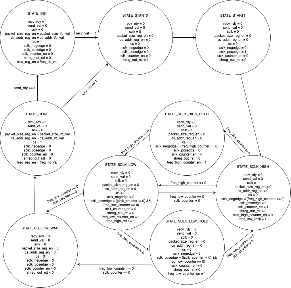
SPI Master FSM for Frequency Division
With the SPI frequency division just completed, this leads us to our current step of adding SPI modes 1-3. Our design before would only follow SPI mode 0. The main changes to allow for the new modes was a set of new cycles for each mode. Each part will have a slight modification. Mainly, the enables for the shift registers and a multiplexer selecting between an inverted and non-inverted SCLK are the new additions to the design. This is planned to wrap up right after Spring Break.
After adding the SPI modes, there is not much else we can add. There is the potential to add a feature for choosing whether to shift the least significant bit or the most significant bit. However, this may be a task for another time as we prepare to divy up our time towards other projects for our third tape-in near the end of the semester.
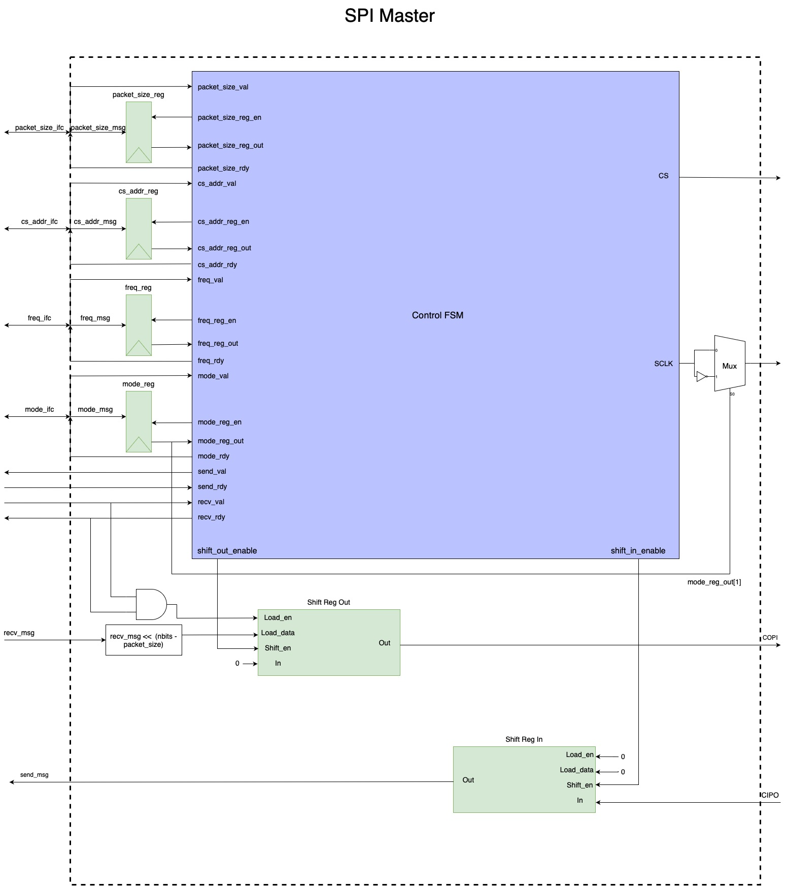
SPI Master Block Diagram with Frequency Division and All SPI Modes
I also wanted to mention the SUNY Poly Nanofab trip that part of the C2S2 team attended on March 26th. Through the connection we had with LaMar Hill, who is a part of NY Creates and DesigNY, we were able to get a guided tour of the Albany Nanotech Complex. This is one of two main research centers for nanotechnology in the world, which brings in different global fabrication companies that are doing research on their own fabrication processes such as TEL and IBM. While we work in the design space of integrated circuits, it is helpful for us to know what happens after we send in our designs for tape-in. Before coming to this trip, I did not have much knowledge on IC fabrication.
First, we were provided an overview of the fabrication process with some wafers showing a finished product of the fabrication process. When we got to walk around the facility, we were shown many of the different machines the facility hosts. Some of these machines were a powerful electron microscope, FOUP transports, and a state-of-the-art extreme ultraviolet machine. While I am sure pictures would be helpful to show what we saw, we were unable to take photographs inside most of the facility. We also saw these machines from a distance since most of them were in clean-room environments.
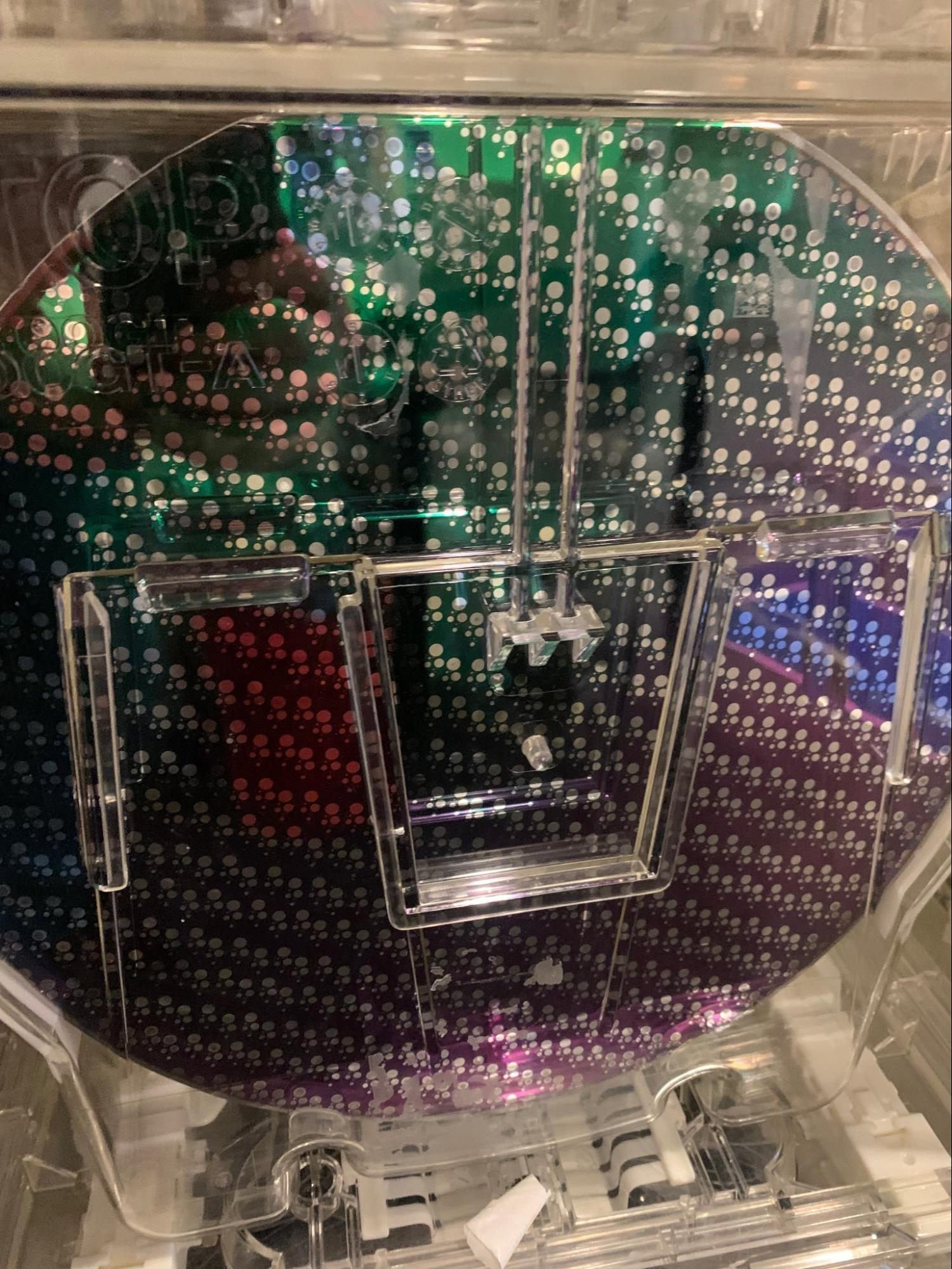
One of the Many Wafers We Saw
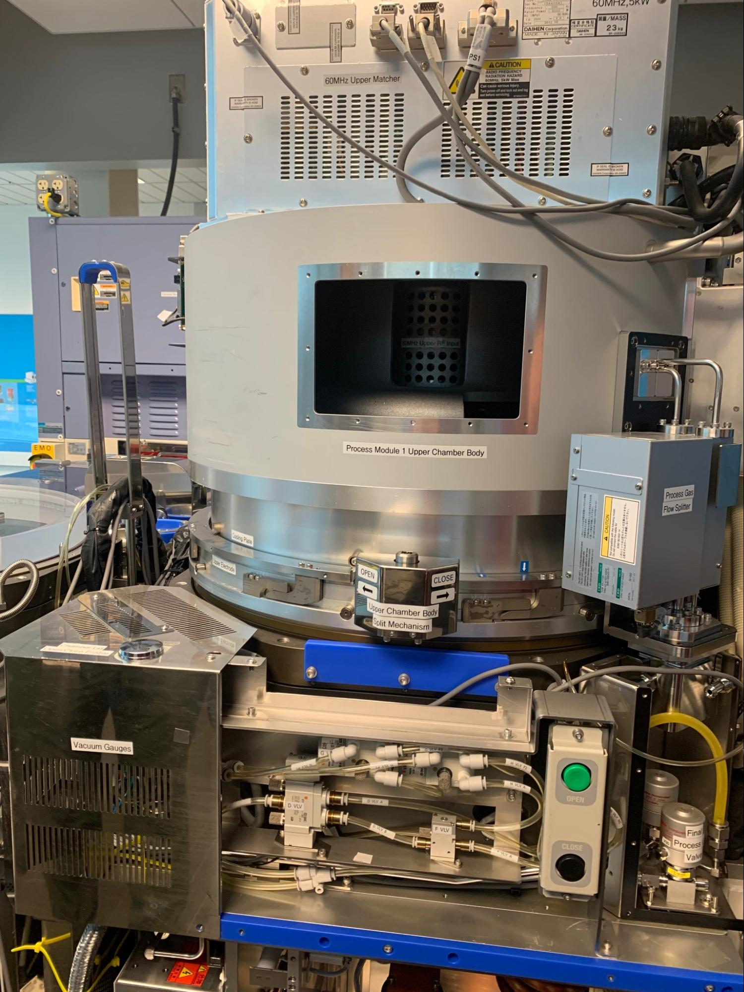
One of the Few Fabrication Machines that We Could Take Pictures Of
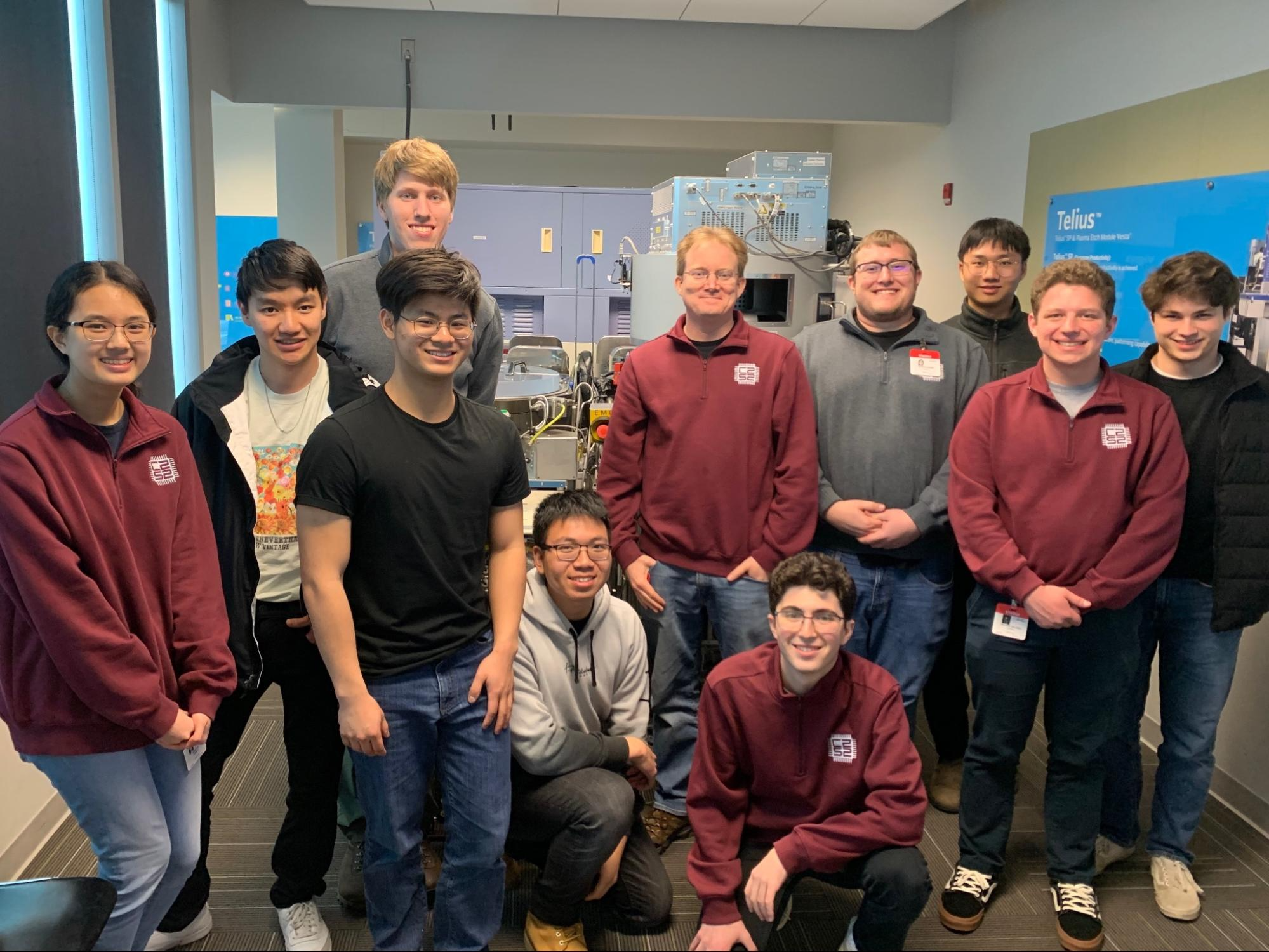
Group Picture of C2S2 at SUNY Poly Nanofab
Truly, it was an amazing experience that I think I will appreciate even more as I dive further into integrated circuits. It has made me consider how I can start learning more about fabrication and physical design. I hope that future C2S2 members can experience the Albany Nanotech Complex.
Hi! My name is Mika Finkman and I'm a sophomore on the digital subteam. I am majoring in Computer Science and planning to minor in Electrical and Computer Engineering. Prior to joining C2S2 in the Fall, I had only taken one introductory computer engineering class, so almost everything I have learned about the area has been on the team. This also means that I focused on smaller projects by myself this year, while assisting Austin with the SPI, mostly taking the time to learn from him and others.
I spent the beginning of this semester wrapping up work on a component I started in the Fall called the SPI arbiter. It was originally designed to allow multiple interfaces to interact with the SPI Master. However, as the digital subteam's design has evolved, so has the purpose of the arbiter.
After finishing the arbiter, the next project I took on was creating a training process for our new members! As C2S2 only started in the Fall, digital subteam members who had little prior experience were only learning from two tutorials created by our team lead, Will. We knew that going into the future we would need a more formal training process if we wanted to recruit new members regardless of their experience level, so that's exactly what I created. The process involves an overview of the digital subteam, brief summaries of prior projects from the Fall, more detailed project papers for optional reading, tutorials created by C2S2 members, and tutorials for basic skills required of digital subteam members (e.g. using GitHub, writing in Verilog, coding structure, etc.).
For the rest of the semester, I have been working with Austin to implement all the changes to the SPI master he described above. This has been very valuable to my experience as a digital subteam member because I had so little experience coming into the team. Getting to learn from someone like Austin has rapidly increased my understanding of so many different computer engineering topics. It just goes to show how collaborative, informative, and rewarding it is to be a member of C2S2.