Progress Report
Will Salcedo and Steven Sun
March 12th, 2023
Hello! Welcome to the first set of blog posts for Cornell Custom Silicon Systems. In this series of posts, we will showcase things about the team that excite us including demos, tutorials, and adventures we have throughout this semester.
My name is Will Salcedo, and I am a senior studying Electrical and Computer Engineering. I'm the Digital Subteam lead on C2S2, and I am responsible for planning digital ASIC projects, designing architectures of digital systems, and supporting our subteam members to achieve a high degree of success. During my time on the team thus far, I have had a blast working with our talented members to develop devices that seem like magic.
In this blog post, I will discuss the overall architecture of our ASIC, some applications, and our tape-in success. We are planning to tape-out our work on the EFabless 2306Q shuttle due on June 5th, 2023.
Due to the release of open-source material such as the SKY130 process design kit, this team is able to exist. A process design kit is a set of standardized gates and rules which allow us to make chips. You can think of it as the set of rules which dictate where you can place the transistors on a chip. We use this set of rules, alongside OpenROAD to automate our transistor placement on the chip so we can quickly explore design spaces without the need for manual design.
The SKY130 PDK is 130nm, whereas modern processes are less than 5nm. Because chip speed and power improve with smaller processes, it is difficult to compete with large companies from a performance standpoint. However, it is possible to compete with modern silicon from an energy efficiency standpoint. Thus, we have decided to pursue applications in energy-efficient architectures, specifically in internet of things (IoT) contexts.
This year, we have been diligently designing a Fast Fourier Transform ASIC, complete with interfaces to a processor and the ability to passively poll a sensor. Shown in Figure 1 is an overview of the intended final implementation of our system. It features three input choices: a microphone for passive sampling, data injection through the SPI Minion, and processor interface for data from software. The system can output data from the SPI bus, or to the processor via the wishbone bus block. This system should allow users to passively collect and process acoustic data from its environment using low power.

Overview of the Fast Fourier Transform (FFT) System Architecture
Figure 2 shows an example architecture of an 8-sample Fast Fourier Transform (FFT). The FFT takes an array of input data and converts it to the frequency domain. The FFT has a variety of different applications in audio processing, radio frequency, computer vision, machine learning, and so on. Thus making it an excellent candidate for hardware acceleration. This is because the frequency breakdown of a signal reveals a lot of information otherwise unknown. The frequency spectrum of a signal can also be used to draw insights about the type of sound being produced. Our Fast Fourier Transform consists of many butterfly units which perform a relatively simple operation.

Overview of FFT Accelerator
Just recently, we submitted a faux tape-out which contained a working model of the system shown in Figure 3. This faux tape-out can be sent to the foundry in the event no other designs can pass the required checks for tape-out on June 5th. We call these test tape-outs: tape-ins. While simple, this design contains the FFT accelerator sandwiched between two SPI Minions. This design allows us to inject and pull data from the system, allowing us to test-run the FFT after tapeout. The implemented FFT accelerator uses fixed-point arithmetic and is eight points. The FFT is pipelined by stage, meaning it can propagate multiple transactions at once. Once the pipeline is fully saturated with transactions, its cycles-per-instruction (CPI) is 32.
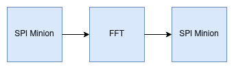
Overview of Faux Tape-Out Design
In Image 1 you can see an image of our hardware accelerator in the context of our tape-in design. This design is about 0.35mm squared. It consumes 350mW of power, and it runs at a clock frequency of 200MHz.

Amoeba Plot of Tape-In Accelerator
We are very excited for tape-out this spring, and we are also looking forward to some of the interesting applications of our hardware accelerator, such as sound identification in low-energy environments. Working on C2S2 has given me the opportunity to work with a rockstar team and the resources to work on complex projects undergraduates would otherwise not have the chance to. I love the interdisciplinary nature of our project, not only amongst technical teams, but also between different applications spaces such as ornithology, meteorology, and other interdisciplinary causes. The digital subteam is working on many other interesting projects, and I hope you stay tuned in over this semester to see more of the cool things we are working on.
Greetings! I'm Steven Sun, a sophomore studying ECE. I joined C2S2 during Fall 2022 as a member of the Digital Subteam, where I've worked on the Verilog FFT project alongside Will Salcedo, Edmund Lam, and Vicky Le. My experience on C2S2 has been very educational, and I've learned a lot about how Python can be used to create testbenches for Verilog files. I am currently taking ECE 2300, and it has been a great opportunity to apply the skills that I learn in class to an actual project.
During my first semester on C2S2, I wrote a Python testbench that took the Fourier transform of a signal using a recursive approach. To demonstrate this testbench, I found audio samples of animal cries and fed them through my testbench. Coincidentally, our campus partner was announced this semester to be a graduate student in the Lab of Ornithology! The details of this partnership are still to be determined, but we know that our FFT will be a critical part of the chip that we design for this partnership.

Fourier Transform of Frog's Ribbit
This semester, I have been focused on creating new test cases for our test script to ensure that our Verilog code has no errors. It is much less expensive to fix errors in software than hardware, so this step is crucial in ensuring that we are making the best use of our time and funding.

Example Test Cases
Now, our testbench is able to randomly generate test cases, which speeds up our testing process and increases our confidence in our FFT.
Additionally, I was able to increase the number of samples per input that our FFT is able to process, and I am currently working on increasing this number by several more magnitudes. To do this, I will be working with Christopher Schiff, who is able to use High Level Synthesis (HLS) to generate Verilog implementation for bit reversal permutation by describing it using high level language. Also, I will be working closely with Edmund Lam to optimize the FFT in terms of power consumption and area requirements.
On March 26th, we plan to visit the SUNY Poly Nanofabrication Facility. Personally, this is exciting because the facility is located 15 minutes away from my hometown, so I look forward to learning about the chip fabrication process in a facility that I've driven past so many times. If this is a good experience, this might be an event that we pursue next year as well! So far, I'm having a blast on C2S2, so I'm hoping you'll still stay tuned to my future posts to see what I'm up to!