SPI Minion, Adapter, and Python Tools
Alga Peng and Xiangyi Zhao
April 16th, 2023
My name is Alga Peng, majoring in Electrical and Computer Engineering. I am finishing my MEng program this semester and am really excited that we are working towards a tape-out this summer.
My name is Xiangyi Zhao, also majoring in Electrical and Computer Engineering and also graduating from MEng this semester. I'm very interested in digital design and computer architecture, and am amazed by what this student-run project team is accomplishing.
We worked here and there throughout the semester and in this post we will talk about several different things that we worked on, and we will be mainly focusing on tape-in 1 and 2 design.
SPI Minion & Adapter
Two of the components to enable communication with the chip are the SPI minion and the SPI adapter. The SPI minion receives and sends messages over the SPI protocol. The MOSI and MISO ports on the left receive and send messages bit by bit, while the pull_in and push_out ports receive and send messages in a whole number of bits.
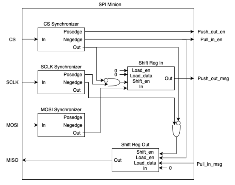
SPI Minion Design from BRGTC5
The adapter converts the pull/push interface of the SPI minion to the latency-insensitive val/rdy interface. Two control bits are added to the beginning of each push and pull message which are used to indicate if the Minion is ready to receive or send more data. The most significant bit of the push message indicates that the SPI Minion receives a valid message; The second most significant bit indicates that the SPI Master is ready to receive the next message from the SPI Minion. The most significant bit of the pull message is used to indicate if the message being sent from the SPI Minion is valid; The second most significant bit is used to indicate if the SPI Minion Adapter has space in its queue to receive another message from the Master.
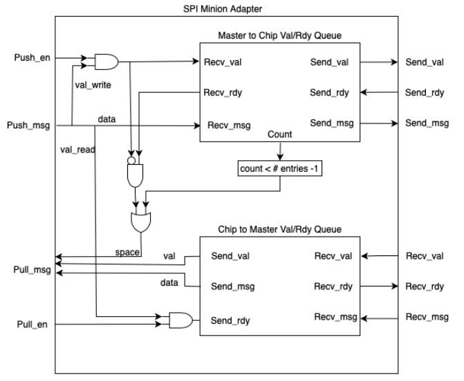
SPI Minion Adapter Design from BRGTC5
SPI Message Auto-Generator
To push messages through the SPI Minion and Adapter, the sclk, cs, and mosi ports must be carefully configured and the control bits mentioned above must be correctly bit-banged to the Adapter before the actual message arrives. Doing this in a manual process is error-prone and unsystematic. With the advice of Will, we made an SPI Message Auto-generator consisting of 3 parts - an input-generator, an output-generator, and a wait-message-generator. The input-generator takes an array of numbers with fixed bit-width nbits as input, and generates an array of bit messages that will go into the SPI Minion ports to send this input array bit by bit. The output-generator generates an array of bit messages that will go into the SPI Minion ports to pull out the array of nbit messages and compare it with the expected output array. The wait-message-generator generates an array of bit messages which tells the SPI Minion and Adapter to wait for several cycles for the inner components to finish the calculation.
To verify this tool, we connect two SPI Minions back to back, so the input array pushed into one minion is expected to be pulled out from the other. We tested different number of elements in the input array for future use - from 1 (for the control messages) to 8 (for the FFT messages).
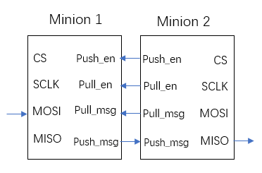
Minion-to-Minion Setup
Tape-in #1 High-level Connection
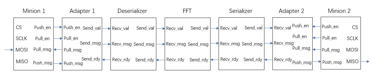
Tape-in #1 RTL Modules Connection
We established the high-level connection for a simple Minion-in-Minion-out flow as shown in Figure 4 above. The first SPI minion receives data from the MOSI line and passes it to the deserializer through the adapter's val/rdy interface. Deserializer and serializer wrap the FFT module to serve as a data format converter. Then the second minion-adapter pair receives the output data from FFT and exports it through the MISO line in the second SPI Minion. This design soon expanded to include other modules and the second minion is no longer needed.
Tape-in #2 Functional-Level Model
Verification is one of the most essential things in most projects, especially for expensive and precise projects such as taping out a chip. We need to be confident that our design works after all top-level connections have been made. Extensive testing is required to verify our design so we mainly focused on the verification part for our tape-in-2 design, which is mentioned and described in Will Salcedo and Steven Sun's post. We worked on the functional-level model for the design shown in Figure 5 (created by Will). The functional-level model structurally represents all the modules shown below and allows the user to test if the RTL model performs as desired. By making a comparison between the outputs of the two models, it is easier to identify the issue in RTL design.
We tested out the functional-level design for different control messages as well. For example, one of the options is to bypass the FFT module by setting the control bits for FFT Input and Output Crossbars. We ensured that if the output selection bit for FFT-Input-Crossbar is set to 1 (the second line) and the input selection bit for FFT-Output-Crossbar is set to 1 (the second line), then the SPI minion should receive the same value as its input value. This indicates that the output is not from the FFT model.
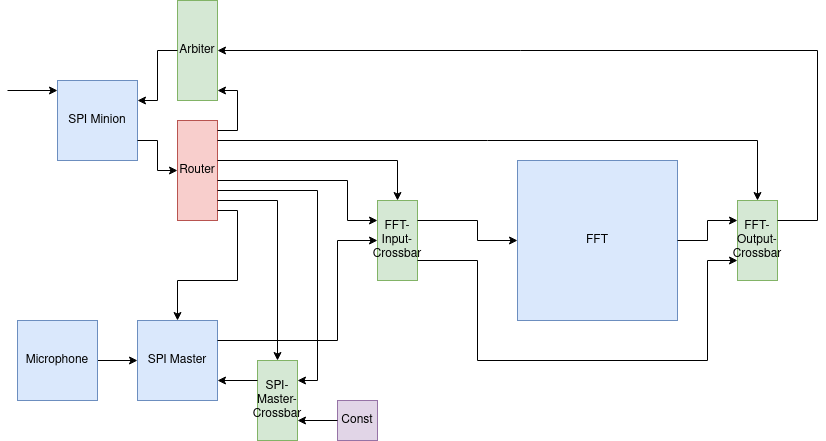
Block diagram for Tape-In #2
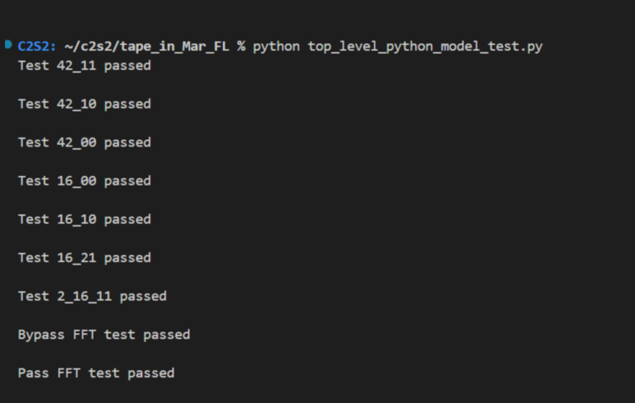
Test Cases Passing for Top-Level Model