Two Sides Of A Coin: How Modules on a Chip Communicate
Tomas Choi and Kevin Liu
April 30th, 2023
What's up, everyone! My name is Tomas and I'm currently in the Digital subteam. During the fall, I was in the Analog subteam. So, I've spent one semester doing analog schematic designs and another working on digital blocks in Verilog. Even though the tools and technical knowledge that I used in these two subteams were completely different, I found both of these experiences to be extremely valuable.
In the Analog subteam, I was assigned the task to design common source amplifiers. At the time, I had no idea what an amplifier even looked like or what common source meant. It took a lot of reading and watching videos to figure out the different equations that applied to mosfets. I used these equations to size the components (e.g. resistors, voltage sources, mosfets) appropriately and obtain the gain wanted. Throughout this process, I learned a lot of the intuitions behind how a change in one part of the circuit affected the other parts. These relationships started becoming natural to me and the design process of new schematics became easier each time. I also learned general sizing guidelines that I implemented into every design. For example, mosfet devices should not be sized too small since they will be susceptible to noise while having a device be too large is not ideal in a chip design scenario. Another guideline was that passive devices like resistors and capacitors should be relatively larger since the smaller the device, the larger the percentage error becomes.
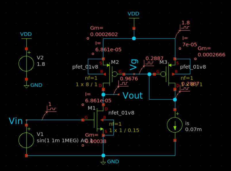
Common Source Amplifier with Current Mirror
In the Digital subteam, I have been working on a blocking crossbar implementation. This was very different work because I was mostly working with Verilog code. Throughout the process of implementing this crossbar, I learned a lot about the care that has to go into writing these modules since anything can go wrong in the real chip if we are not too careful in the design phase. One of the strategies to ensure correct data processing was the latency insensitive val/rdy protocol. The purpose of this protocol is to actively communicate with connected blocks to ensure that the block is outputting the correct data. Any input or output message will have its own valid and ready bit. An input message will be successfully sent from a previous block to the crossbar if the block sending that message says it is a valid message and if the crossbar itself says that that input port is ready to receive a message. Output messages work similarly, but, instead, the crossbar is the one outputting the valid bit while the block coming after it will tell the crossbar if it is ready to receive the crossbar's output. These protocols are extremely necessary for the chip functionality to come out as intended.
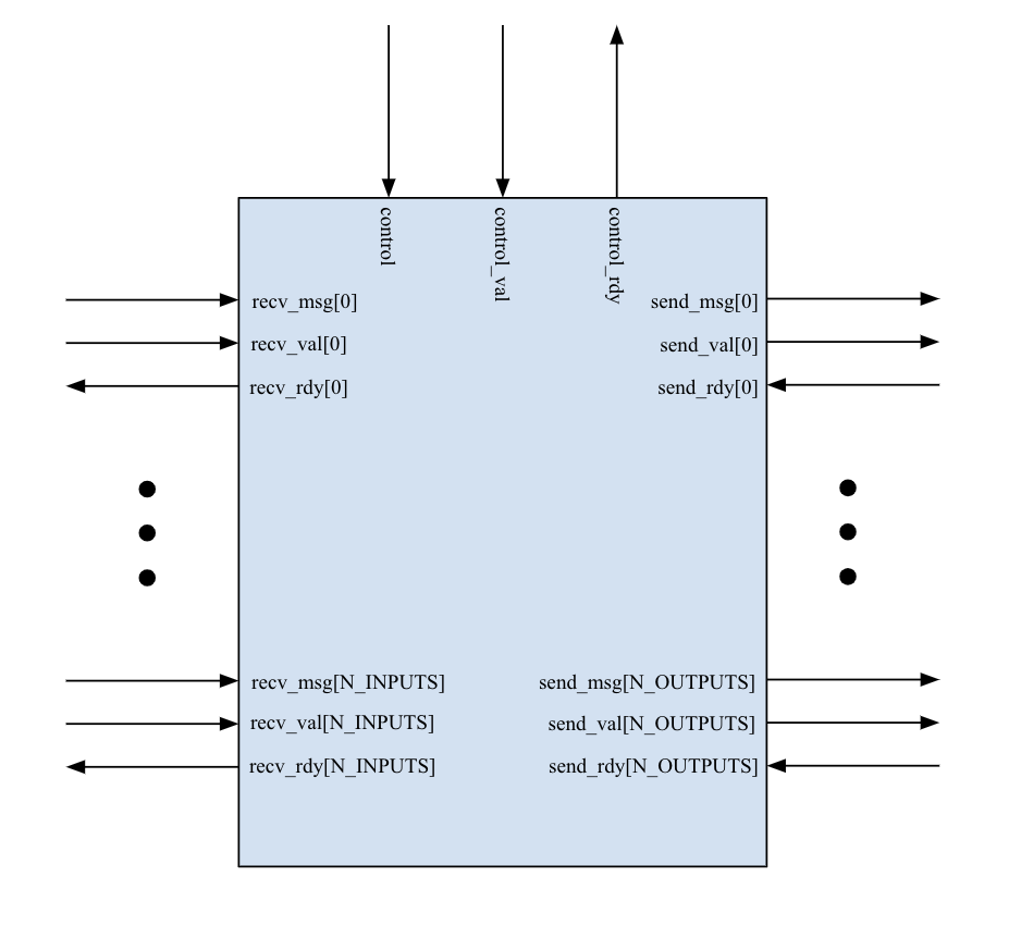
Crossbar Block Diagram
One of the reasons I applied to C2S2 was that I wanted a source of 'accelerated learning'. I was very eager to learn and solve all the mysteries that were bothering my mind regarding topics in ECE. I thought that if I took classes while simultaneously being in a project team that applied those topics, I would learn at a rate faster than anyone else. In C2S2, I was able to experience this 'accelerated learning' in two different forms. For the Analog subteam, I used the design experience from C2S2 to better understand the applications behind the physics behind semiconductors information that I learned in Microelectronics class. For the Digital subteam, I applied the theoretical knowledge behind combinational and sequential logic blocks that I got from Digital Logic class into its Verilog implementation with timing and data loss constraints in C2S2.
Hi, I'm Kevin Liu, one of the new C2S2 members and the youngest member on the Digital subteam. I plan to pursue a double-major in CS and ECE, and am passionate about application-specific silicon design as a potential career path. Currently, my project heavily involves how messages are sent between different modules of a chip, so I will be sharing some of the ways that this can be accomplished.
My project involves using the Wishbone Bus, an open-source bus design that has the potential to be very useful on the C2S2 chip. If used on our FFT accelerator chip, it could, for example, allow much easier input of the FFT commands to the chip with less precise timing and latency requirements. For now, I am in the process of building and simulating a simple proof-of-concept module for the Wishbone Bus that will allow us to test and explore its behavior.
The Wishbone specification is a handshake-based read/write cycle protocol where a master sends read/write instructions to a slave, and the slave sends an 'acknowledge' signal once it is done processing the instruction. This ensures that the master never sends instructions too fast for the slave to process. A diagram of the Wishbone interface is below. The Caravel harness includes a Wishbone bus master, so I am creating a wishbone slave that will act as an interface to a first-in-first-out (FIFO) queue. Writing to this module will add data into the queue, and reading will extract from the front of the queue. This will allow meaningful testing of read/write functionality.
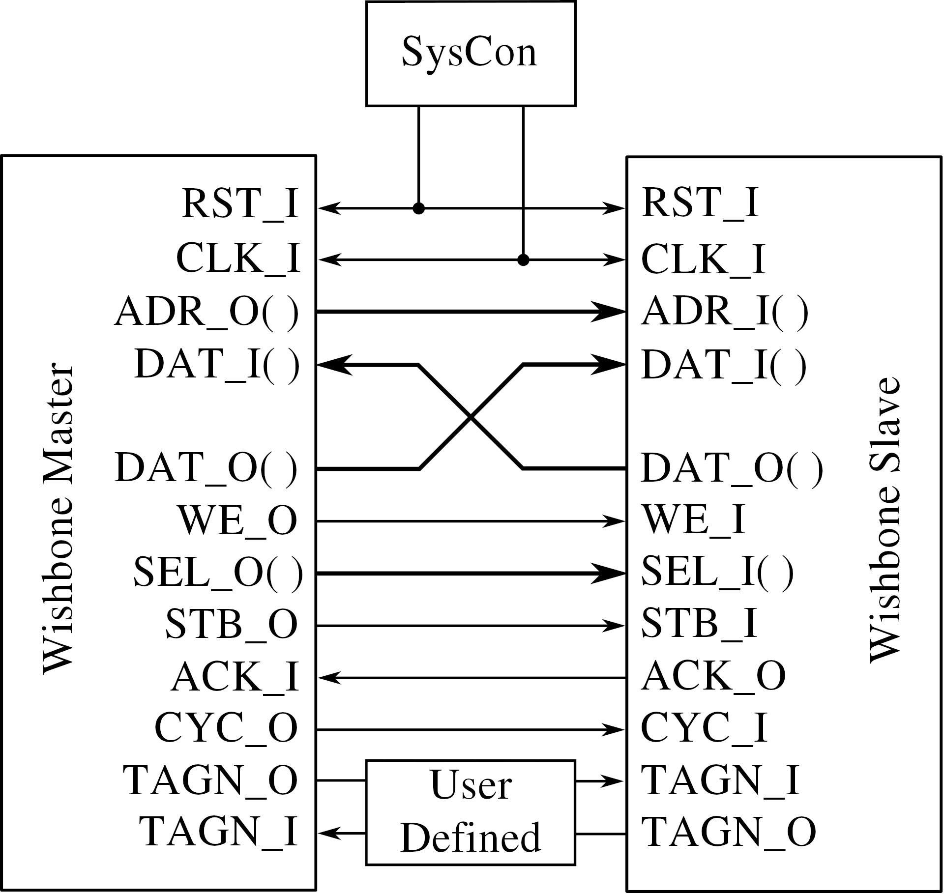
Wishbone Interface
The queue uses a different communication protocol, called the val/rdy stream interface (meaning 'valid' and 'ready'). The protocol connects a sender, which controls the valid signal, and a receiver which controls the ready signal. Every cycle, the sender sets the valid signal to high if it is sending a valid data message along the data line. The receiver also sets the ready signal to high if it is ready to receive a message from the data line. Both the sender and the receiver monitor both signals, and when they detect that both are high, the message is considered to be successfully sent. Otherwise, if only the valid signal is high, it means that the sender is sending the correct data but is waiting for the receiver to be ready for it. If only the ready signal is high, that means the receiver is ready for a message and is waiting for the sender to send one and mark it as valid.
The Wishbone queue module needs to use two val/rdy interfaces: one for the queue to receive data (with the wishbone as the sender and the queue as the reader), and one for the queue to send data (with the queue as the sender and the wishbone as the reader). The former is through the ports prefixed by 'recv', and the latter is through the ports prefixed by 'send' on the queue, and all the connections of my module are shown in the block diagram below. Most of the design of my module involved combinational logic to connect the wishbone interface with the val/rdy interfaces appropriately.
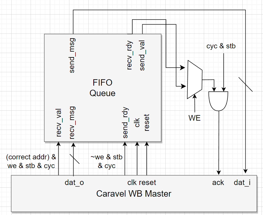
Block Diagram of Wishbone Block