From Idea to Chip: ASIC Design Flow
Kevin Rodriguez and Vicky Le
April 28, 2024
Over the past 2 years, C2S2 has worked on creating ASICs to provide undergraduate students with experiential learning opportunities in chip designing while also working to give back to the community by designing the chips to help the Lab of Ornithology. But what exactly is an ASIC and what is the process from idea to getting the chip back?
In this blog post, we will be explaining what an ASIC is, parts of the ASIC flow, and how C2S2 has worked through the ASIC flow.
What is an ASIC?
ASIC stands for Application Specific Integrated Circuit and are chips designed with a single purpose. Unlike general-purpose integrated circuits, these chips are designed to optimally perform a single task which leads to many benefits including a smaller footprint, lower power consumption, and higher performance than other general-purpose devices such as FPGAs that can be used for many tasks.
As a result of these benefits, ASICs have a multitude of applications in many industries and can be seen in everyday life. Custom chips can be found in cell phones, digital watches, toys, cars, and other devices to control how the device will function. From this short list of applications, it can be seen that ASICs are used in telecommunications, automotive, entertainment, and many other industries.
What are the Design Steps to Create an ASIC?
The ASIC design flow is the process that is followed to go from the idea to having the GDS file to be sent to the foundry to fabricate the chip. We have broken this design flow into the following 9 steps in this blog post. The figure below shows these 9 steps in addition to the categories which these steps can be divided into. In red are the steps related to creating the register transfer level (RTL) design. Following this are the steps in green which is the logic design phase, and after the logic design phase is the physical design phase.

Design Specification
To begin a project, the design specifications, including the chip's purpose and the device's intended operation, need to be specified. Specifications include defining the functionality of the created chip, inputs and outputs, performance, space, and power consumption, and these specifications are followed throughout the design process.
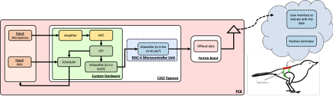
Within C2S2, design specification was completed while speaking with our campus partner, the Lab of Ornithology, to determine their wants and needs for a custom bird tag such as being low-power, compact, able to collect audio data and bird movement, and configurable to change settings such as when to collect data. Following speaking with our campus partner we specified that being low power to extend the battery life of the bird tag and having a microphone and accelerometer are the main requirements of the system produced to fit the campus partner's needs. Below is a diagram showing the end goal of the created system and how it will be used. Furthermore, the white box labeled C2S2 tapeout shows where the created chip(s) are and their purpose in the data flow and overall system. In this system the yellow boxes denote the analog team's chip and the green specifies the digital team's chip, and for this blog post we will focus on the digital team's view of going through the ASIC design flow.
RTL Description
Register transfer level (RTL) description is the next step after design specification. At this step, the high-level abstraction of the digital circuit is created using a hardware description language (HDL) such as Verilog or VHDL. In practice this is when designers define the operation of the system, create data paths, and write the control logic to achieve the desired functionality of the chip. One thing to note at this step is that this definition of the operation of the chip does not involve focusing on the physical implementation of the system such as the layout of transistors or routing of interconnections, but rather on writing the digital logic of the design.
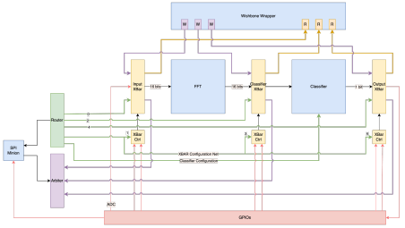
While working on C2S2 this design step looks like writing Verilog to specify the data flow and creating the modules as seen in the system architecture diagram of the digital team's tapeout this year. Once the modules are created the system is connected to create a system composed of the different submodules.
Functional Verification
After writing the Verilog for the system and connecting the modules, the system is tested for functionality by writing test benches that simulate having different inputs given to the system and comparing the outputs to what is expected.
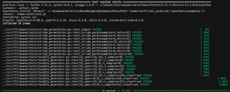
On C2S2 we complete the functional verification stage by writing PyMTL test benches to check for correct outputs given different inputs including what happens when there are delays and different types, combinations, and values of inputs. At this stage, the goal is to test all possible cases and ensure that the functionality for these tests is deterministic and reproducible. The figure below shows some testing completed for the FFT module of the system.
Logic Synthesis
Following testing of the functionality of the design, the RTL design is transformed into a gate level netlist through logic synthesis. Logic synthesis can be broken down into 3 steps including translation, optimization, and technology mapping. During translation, the RTL code is translated into boolean equations (technology independent synthesis), and these boolean equations are then optimized using optimization methods such as sum of products (SoP) or product of sums (PoS). After optimizing the boolean, the boolean logic is then mapped to logic gates (technology-dependent synthesis). This process of mapping boolean logic equations to logic gates in the target standard cell library is dependent on the technology being used to tapeout the chip.
Within our team the steps of logic synthesis until our GDS output is done by pushing our design through OpenLANE, to harden and synthesize our design.
Gate Level Netlist
Once the logic synthesis is complete, Caravel generates gate level netlists for our design. For starters, a gate level netlist is a low-level description of a circuit that contains all of the primitive circuit instantiations and their appropriate connections. The netlist is stored in a Verilog file, but although it looks like a typical module, it only defines variables and connects them, and does not actually have any functions. Gate level netlists provide us with an alternate form of testing, which we can use towards the end of our flow to observe and manipulate signals in specific wires. These netlists are also foundational to the further checks that Openlane carries out.
Logic Equivalence Check
Once we have our netlists output from logic synthesis, Openlane performs checks on the timings of signals, making sure that they fall within specifications. Openlane does this with OpenSTA, which is an open source gate level static time verifier, which is fed the design netlist with a configuration file. In the config file, we declare the clock period and the amount of "slack" the chip has in its setup and hold time, indicating the amount of time the chip must hold its signal before and after the clock period. OpenSTA then outputs timing reports, with detailed information on whether each signal successfully fell within appropriate times, or how much time they were off by. An important factor involved in this process of the flow is the clock period of the circuit, therefore this step gives us a good indication of how well the clock period is allowing the signals to flow and if we need to slow it down or we can speed it up.
Place and Route & Physical Layout
Once it has been verified that the design fulfills all logic tests, meaning functionally our chip is behaving how we want it to, Openlane begins to physically 'lay out the pieces'. Still, as stand-alone blocks our modules are basically useless in the real world, which is why it is placed on the Efabless Caravel harness. The harness is basically a chip which supports basic functions, such as IO, power, and an SoC (System on Chip) core, and provides us with a user project wrapper where we can place all of our modules within an allocated area of 3000um x 3600um.
Openlane does this process with OpenROAD, an open source tool that provides flow scripts for the process of actually putting things on the physical chip design. This can be broken down into roughly four major stages: Floorplan, Placement, CTS, and Routing. All of these stages have many MANY steps that go on behind the scenes that are crucial to the flow, but it is still important to understand the basic idea and goal of each of them. Floorplan starts us off by defining the area the chip is going to take up and creating the power distribution network that all our components will work with. Placement places our macros where we have specified them to be, and also places all our cells and optimizes such placement with regards to factors such as slew, capacitance, and wire length. CTS or Clock Tree Synthesis identifies high-fanout nets, or connections that indicate a lot of loads, and resizes and places buffers accordingly in order to distribute the clock network. Lastly, Routing is the stage in which all modules are connected appropriately, ensuring that basic time and power violations do not occur.
Physical Verification
Right before the final results are outputted, Openlane undergoes various signoff processes that ensure the chip meets all physical requirements. This includes DRC checking, or Design Rule Checking, which verifies that the design meets the constraints of the technology involved in its manufacturing. Still, this does not guarantee that it represents the circuit we wish to fabricate, which is why alongside other verifications, Openlane also performs an LVS check, or Layout Versus Schematic check. As the name suggests, it compares the layout to the original circuit schematic, ensuring consistency through the hardening process. This is done by comparing the netlists of the circuits and asserting that they match.
GDS
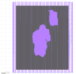
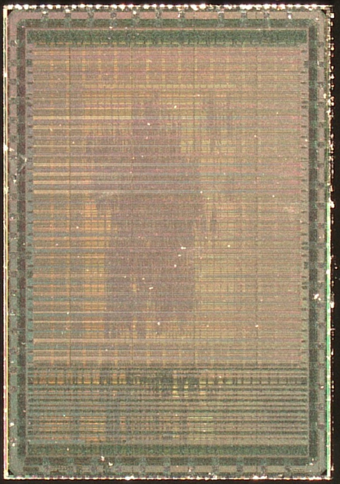
Lastly, our final output for the process is the GDS file. This file stores information about where everything is physically located in each layer of the final design. This is the final product of the chip design process, and it is what we send to the foundry in order to have the chip physically constructed. The figure below on the left gives a visual representation of the GDS file and the figure on the right is a picture of the digital team's chip from 2023.
Conclusion
The ASIC design flow is a multistep process that involves designers at all steps of the process from idea to getting a chip and although this process can be difficult and long, going through this process yields a chip that can greatly improve the performance of a system and opens the doors for innovation and unparalleled efficiency.
We hope this blog post has given you a better understanding of the ASIC design flow and insight into a real experience going through this design process. From working on C2S2 it has truly been a cool experience to go through each of these steps and see how a chip can be designed from an idea to having a tapeout and getting the chip back.