GDS Chip Art
Emily Lan and Demetrios Gavalas
March 24rd, 2024
This blog post was inspired by jazvw and uses code from them! It can be found at https://github.com/jazvw/chip_art and all rights surrounding the code belong to them.
Intro
GDS art is a great way to give our custom chip some flair! More importantly though, learning how GDS art is generated can give us some good insight into what GDS is, and how it is used to go to the high level designs we are familiar with to actual fabrication of our custom chips.
On Layouts
The Integrated Circuit (IC) boasts a compact yet complex architecture. At the heart of every IC lies its layout, or the IC mask layout, which delineates the arrangement of metal layers and interconnections of the circuit in a geometric and three-dimensional representation. At its heart, it serves to detail the functionality and performance of the IC.
Those area lot of words. We prefer to call it a complex digital soldering experience. Gross oversimplification? Maybe. But allow us to explain:
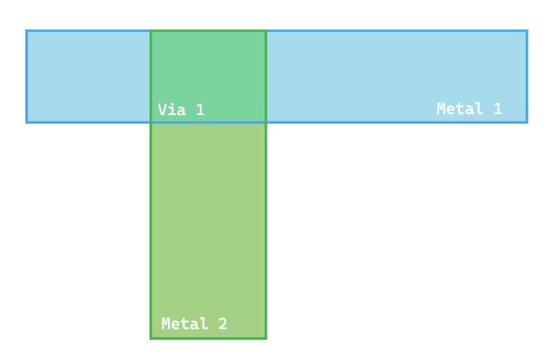
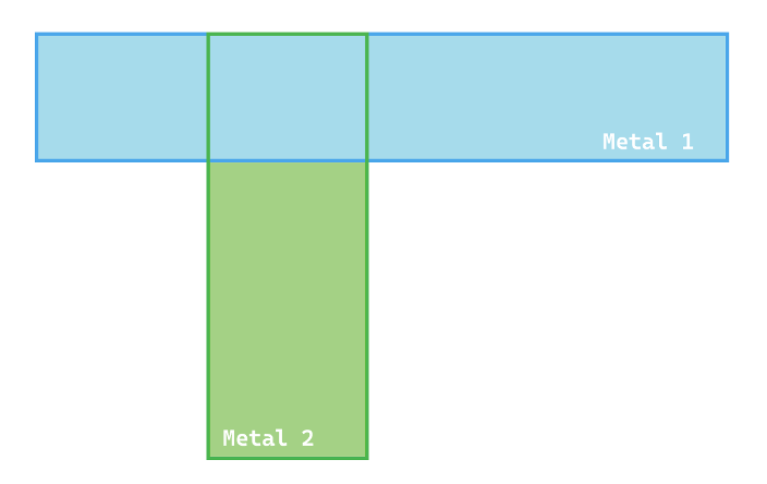
In order to connect two devices together in a layout, you link them together with a layer of Metal. If you'd like to connect those two Metals together, (thereby linking those two devices together as well), you link them with a Via where they intersect. See? Just like soldering.
Of course, digital layout design is mostly automated these days, especially with how big these ICs are, and you don't really get the opportunity to do this yourself unless you'd really like to.
Still, there are opportunities to get up close and personal with layout design.
We need to first understand the building blocks of a layout: LEF and GDS files.
LEF and GDS Files
There are two kinds of LEF files: Cell LEF files, and Tech LEF files.
The Cell LEF file contains the layout information for a single cell on your board. It contains a cell name, class, sizing and symmetry information, and pin information. This allows the layout to be separated into discrete cells, which improves organization and modularity.
Tech LEF files contain information for all of the metal interconnects on a board, including their geometry and physical dimensions. These are specified layer by layer, in process order, meaning that the LEF file is specifying how each layer is actually being fabricated.
GDS files are a kind of database file which are used to store the full three-dimensional layout of the chip. That's what you send to a foundry, which is how they configure their machines to make your chip. Like LEF files, the making of a GDS file is mostly automated using high level tools. While they generally describe functional parts of the chip, we can also use it to put more fun stuff on our trip, like art.
GDS Art
Now that we understand GDS and LEF files, the idea of GDS chip art becomes very, very possible!
At its core, we're taking pixels-a bitmap, to be more precise-and mapping prominent geometric shapes with different layers of metal. Different colors utilize different layers of metal. Vias aren't necessary, because we aren't looking for functionality out of this thing-just that it looks the way we want it to!
The code involved in making this process possible is a little more complicated. We used jazvw's code, which can be found here, in order to transform our PNG into a GDS file!
One thing to note: while we went through the process of exploring jazvw's code and using it in order to transform it from a PNG into a GDS file, we noticed that there was an issue with the python environment. In order to get the script up and running, we went into the makefile and changed ./chip_art.py to python3 chip_art.py. This uses the Python3 environment rather than Python in our path, which solved the issue. If you don't have this issue on your end, great! If you have it, it's something you can try.
You'll also have to tinker with the image width a little bit, as that's something you have to specify when taking your picture from a PNG to a GDS file. You'll want to change your PNG picture width to the specific amount of pixels you'd want your GDS to be in µm.
We decided to use the C2S2 logo for our expedition into GDS art. This is a relatively simple transformation, visually speaking; there are only two colors involved in our logo. And, sure enough, here's our final result!
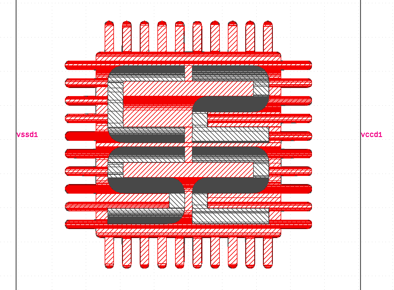
Isn't this super cool???
Now, how did we open this file? GDS files aren't exactly readable on their own.
Opening a GDS File
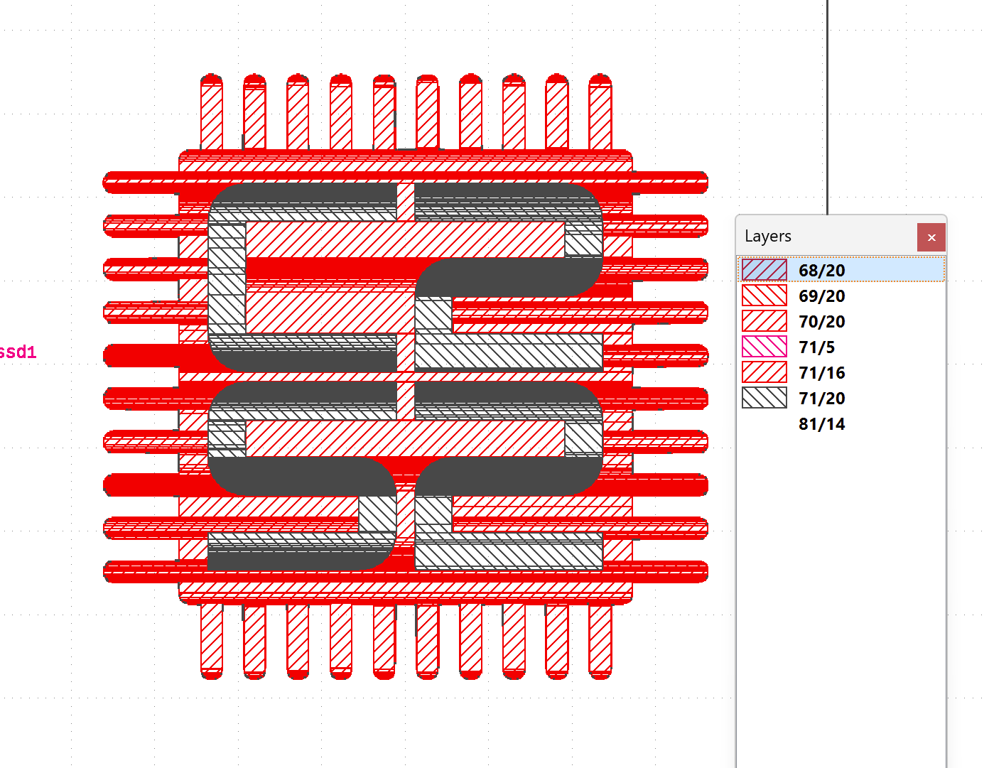
We used Klayout in order to open our C2S2 logo, which seems to be the most reliable and user-friendly open-source application capable of opening and viewing a GDS file!
Klayout allows you to draw your own layouts, view layouts (like we did for the logo), and handle GDS files in a way that would otherwise be super, super difficult without exclusive industry tools like Calibre DESIGNRev.
Therels also Gdstk, a C++ library that, in its own words, is meant "for creation and manipulation of GDSII" files! It's definitely worth checking out if you're going for further customization and creation of your own GDSII files.
Now you can try on your own!