Room at the Bottom: Imaging Silicon
Daniel Kaminski and Caden Xu
April 28, 2024
Process Node Progression
Ever since the first integrated circuit was conceived (more than 60 years ago), "Moore's law" has been matched by the progression of process nodes. The law states that the amount of transistors on a chip doubles every two years, leading to an exponential increase in computing power, and the multibillion transistor chips we enjoy today1. Improvements in semiconductor technology have led to decreases in feature size, allowing for this increase in transistor count. As a result, imaging chips has become ever more difficult, as modern 5nm or 3nm process nodes require powerful scanning electron microscopes to see the smallest features.
However, the Skywater 130nm process node that C2S2 uses is large enough that while the smallest of features cannot be seen with an optical microscope, larger components, such as resistors, capacitors, top level interconnects, and some transistors, can be seen. This blog post discusses images taken of C2S2's analog and digital tapeouts from last year. Additionally, we also imaged an Atmel Mega 1284, which uses a process node large enough that most features, even digital standard cells, can be seen optically. With regard to the speckling seen in the microscope images, it is due to a fault in the microscope camera, and should be disregarded if possible. With that being said, let's begin with a look at C2S2's digital tapeout from last year.
Digital Chip: Eagle
Prior to tapeout and manufacturing, we were able to see a top level view of the digital gate placement using layout software, such as Klayout. Rather than painstakingly hand placing thousands of digital logic gates, we designed these chips with the Verilog language, which was then synthesized, and converted to a GDS file with place and route software. The cluster of gates present in the amoeba plot below shows the general location of the standard cells and interconnects on the chip, as viewed digitally prior to fabrication.

Amoeba Plot of "Eagle" Digital IC (FA23 - SP24)
Out of curiosity, we decided to explore how our design actually appears on silicon after fabrication with an optical microscope. By imaging the bare die, we discovered a few interesting easter eggs and features that are visible only after fabrication. Shown below are images of the digital chip, codename "Eagle,"" under a microscope.
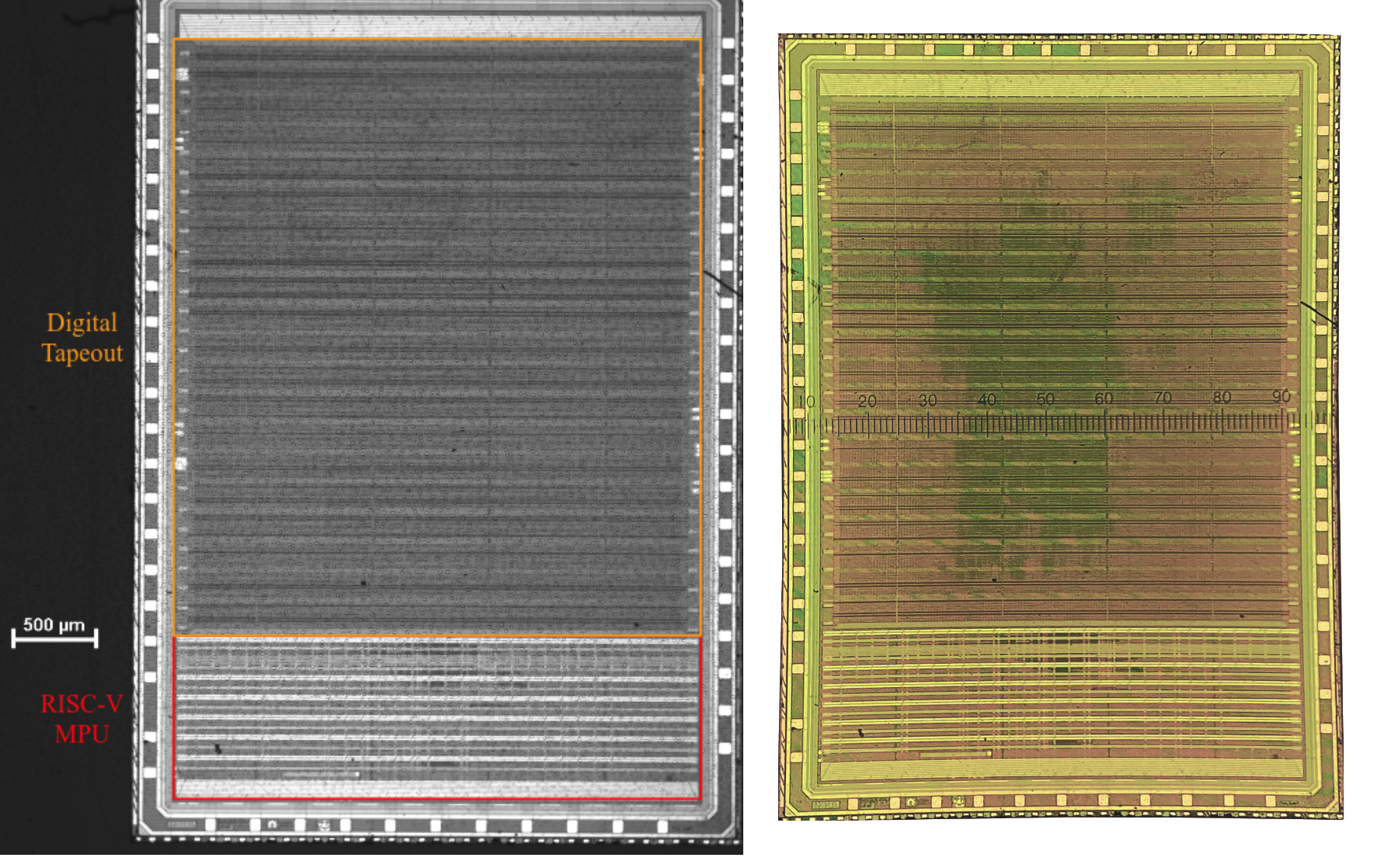
Annotated Microscope Image (left) and Phone Camera Image (right) of Digital "Eagle" IC (FA23 - SP24)
Initially, the view of the digital chip was uninformative, as metal ran across the chip in its entirety, in an almost mesh like pattern. This effectively shrouded smaller transistors and other interconnects that were lower than the top level metal layers. This was exacerbated by the monochrome camera present on the microscope being unable to capture subtle variations in color.
Fortunately, after careful inspection of the chip, some similarities between the amoeba plot and the manufactured die emerged. To capture these features, a color photo was taken with a phone camera using the microscope eyepiece, which was then digitally enhanced. On the right, the green "blob" present in the color photo has considerable similarity to the amoeba plot in Figure 1, indicating the locations of the gates. On the bottom of the chip we identified a RISC-V processor. This component was added by our manufacturer, Efabless, and facilitates pin assignments, serial interfacing, and other external and internal communication.
After increasing the magnification of our microscope, we can begin to see more interesting features.
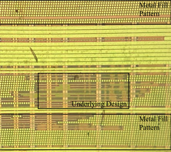
Microscope Image of Metal Fill Pattern
One of the most striking differences between the original and fabricated design is the presence of many metal squares which exist on not only the top metal 5 layer, but on lower layers also. This is likely evidence of a technique called metal fill, which is added to improve the reliability of chemical mechanical planarization (CMP)2. During CMP, the wafer is polished abrasively to flatten the metal and oxide on each layer, before depositing the next layer. These metal squares are added to ensure that the wafer is flattened uniformly and to prevent "dishing,"" as metal and silicon are abraded at different rates.
Analog Chip: Sparrow
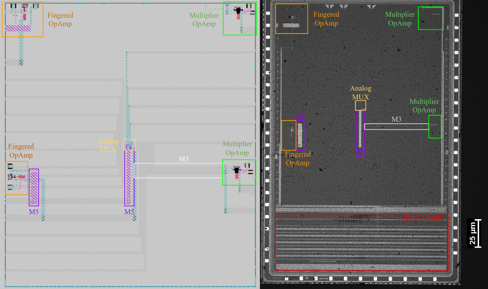
Annotated Magic VLSI View (left) and Microscope Image (right) of Analog "Sparrow" IC (FA23 - SP24)
The analog tapeout for last semester focused on the development of two types of operational amplifiers, fingered and multiplier. The fingered design utilizes MOSFETs with multiple passes of polysilicon over the diffusion, whereas the multiplier MOSFETs are simply several identical transistors, with metal connecting the diffusion contacts. However, differentiating the two would require zooming further into the image - in this blog post the focus will be placed on the top level image.
An analog multiplexer sits in the middle of the die, which selects signals from the two vertically centered opamps that are output at the chip IO. The top left and top right opamps are connected directly to analog IO pins, so no multiplexing is required.
Similarly to the digital chip, the analog chip, codename "Sparrow," contains a RISC-V MPU, which can be seen when the die is viewed through the microscope. In the case of the analog chip, this MPU is mostly used to make IO assignments, which allows us to enable the analog MUX.
Unfortunately, much of the view of the design is obstructed due to the metal fill layer, as is the case with Eagle. Some bright shapes can be seen in the microscope image, and generally can be visually matched with the corresponding components seen in Magic VLSI. Metal 3 and metal 5 layers can also sometimes be seen as thick white stripes, such as the metal 5 layer running alongside the multiplexed fingered opamp.
Due to the small size of the standard cells used for the analog multiplexer, as well as the lack of resistors and other large components in that area, it is quite difficult to see in the microscope image. However, the area where it is located is highlighted in yellow, which can be estimated using the location of the metal 5 layer running to it.
ATMEL MEGA 1284
For fun, we (destructively, and with pliers) disassembled an ATMEGA 1284 microcontroller - our copy of which was produced in 2009. This microcontroller had three visibly distinct sections: analog, digital, and memory. The memory in the chip is split into 16 KB SRAM, 128KB Flash, and 4KB EEPROM3. However, since flash memory is densely packed, and very repetitive in its design, it is likely that the memory block shown in Figure 5 is Flash memory. Unsurprisingly, its large capacity relative to both the SRAM and EEPROM causes it to take up more space on the die than the other two forms of memory.
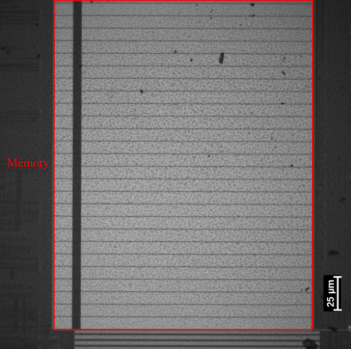
Annotated Microscope Image of Atmel MEGA 1284 Microcontroller Memory Module
Moving onto the other two sections, their boundary can be clearly seen in Figure 6. Here, the sea of gates technique, likely synthesized from a hardware description language, is applied to the digital section (seen on the right). The analog section, which encompasses the ADC, analog comparator, and voltage reference, can be identified by the presence of large passives such as resistors and capacitors, distinct to an analog design.
Additionally, the manually sized transistors, and the unique, handmade pattern of this region indicates analog design.
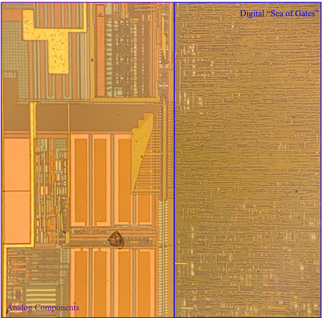
Microscope Image of Atmel MEGA 1284 Microcontroller Analog Portion (left) and Digital "Sea of Gates" (right)
Wrapping Up/Chip Art!
While reading this blog post, some of the keen eyed among you may have spotted something interesting at the bottom of both the digital and analog tapeouts. If you didn't notice anything, scroll back and see if you can find it.
Chip design does not have to be limited strictly to engineering - it encompasses art4. Below are some examples of the silicon designs present on Eagle and Sparrow chips, which are only visible when viewing the chips with a microscope. More likely than not, there is a piece of silicon art on the processor that runs the device you are using right now. We hope that in the future, our tapeouts can also come to include chip art, connecting art and engineering, forever on silicon.
We would also like to thank the Cornell Nanofabrication Facility (CNF) for access to microscopy equipment, without which this blog post would never have been possible.
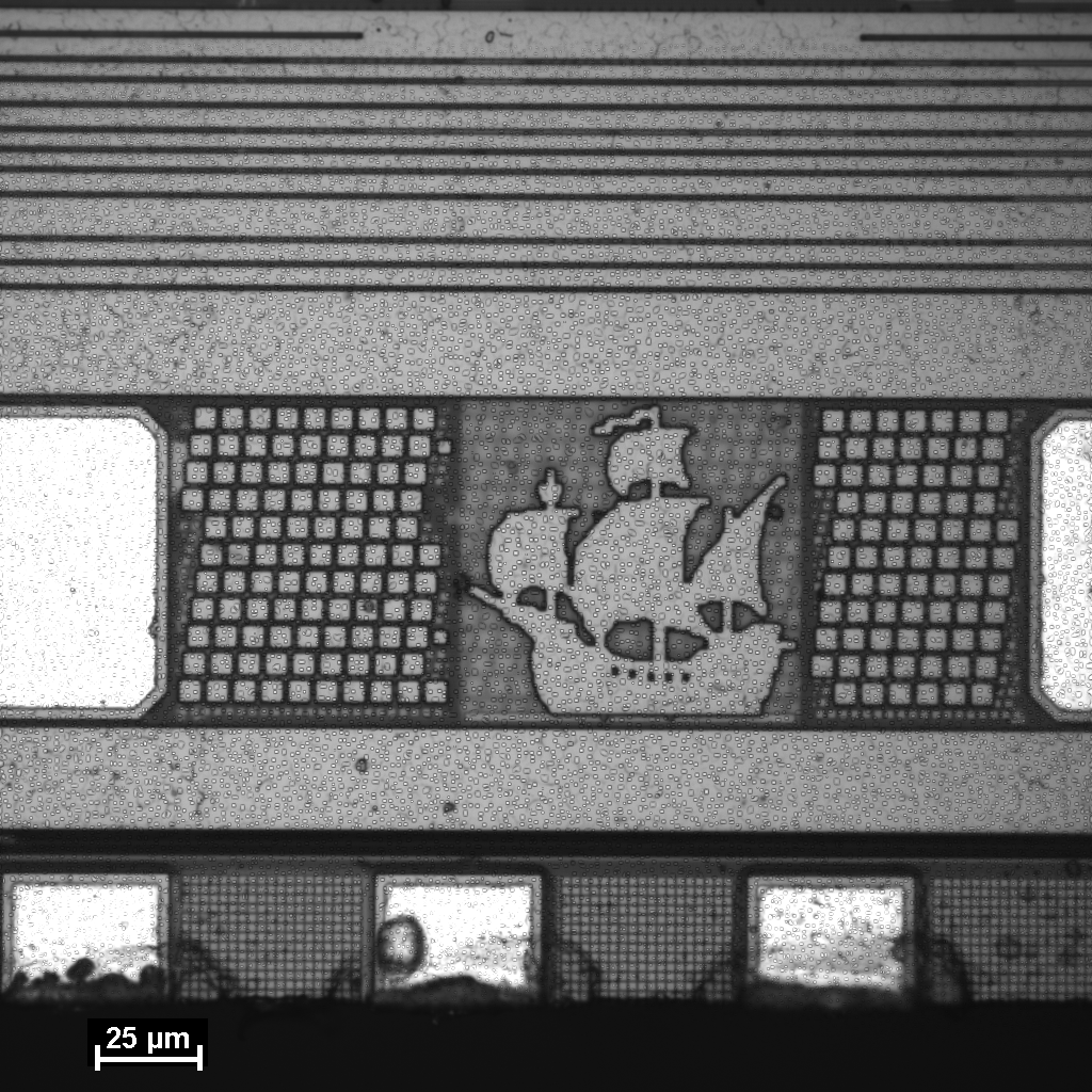
Microscope Image of Digital Chip Art (Ship)
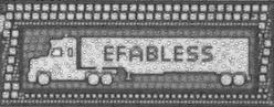
Microscope Image of Analog Chip Art (Efabless Truck)
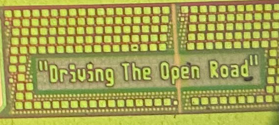
Microscope Image of Analog Tapeout Chip Art ("Driving The Open Road)
References: