Doing Magic in Magic VLSI
Thomas Figura
April 24, 2024

http://opencircuitdesign.com/magic/
In C2S2 on the Analog Subteam, a key tool that we use in the process of tapping out an IC is a tool called Magic VLSI. Magic VLSI is a layout tool created by John Ousterhout and his graduate students at UC Berkeley in the 1980s. While Ousterhout no longer maintains this project and although it was created almost 40 years ago, Magic VLSI remains a crucial component of Open Source Layouting. Thus in this blog post I will create a Magic Tutorial that will hopefully help you layout and extract your very own integrated Circuit.
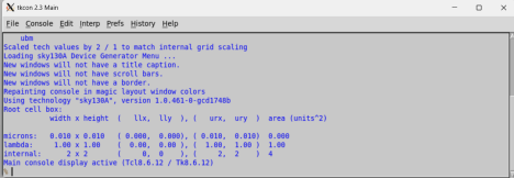
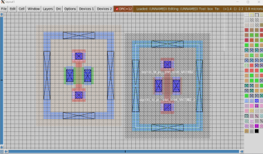
To begin, Magic is primarily run through the command interface window (CIW) as shown above. With the visual window, shown below, being used for visual inspection. Mouse support for Magic has been added overtime but for most features, the CIW remains king.
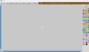
From this visual interface we can see how Magic looks, firstly we have the window on the right. This window shows which layers are available to you through the loaded PDK, in this case that PDK is Skywater 130. Next at the top of the screen all of the expected tabs plus some new ones are there. In File you can open a magic file, save a magic file, import a spice netlist to generate cells, read and write a GDS file, and close Magic. In Edit, you can manipulate cells through rotation and shifts. In Cell you are able to place instances and move throughout the hierarchy. In Window, you are able to modify the Visual window above. Layers allows you to lock and unlock layer modification. DRC gives you access to drc commands. Options allows you to access more Magic options that for me personally haven't been used. Device 1 & 2, allows you to generate Skywater130 PCells.
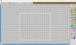
With that out of the way we will begin with the generation of a simple Magic layout, in this blog post we will be going through a simple CMOS inverter. To begin we first need to set up the Magic environment to be the most helpful. In Magic everything that is done is through the use of the "box", the white outline in the above photo. This box is changed by left and right clicking, where left click moves the bottom left corner and the entire box with it, while right click moves just the top right corner. Thus we run these commands in the CIW to begin:
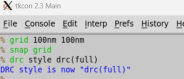
This is done so that we have a visible grid to work with and that our box is locked to said grid. The DRC command is done so that the DRC deck is fully initialized, just in case it is not.
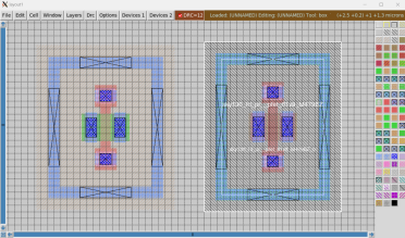
From here we are going to create the inverter, from Device 1, we select nmos, then create and close, then away from the created device and do the same with the pmos. From here you will most likely have an image like:
Where the cells are not exactly aligned and where you want them. To overcome this you select the cell by hovering over it with your mouse and press I, this selects the cell and allows you to do actions on them. Once the cell is selected you can then press M to move the cell from the bottom left, or you can hold M to drag the cell.
Now that we have moved the cells to be more aligned with each other we noticed the big red 12 DRC errors at the top of the screen. Magic in real time checks the layout for any DRC errors, and in this case has spotted that the initial metal layer on the gates is too small. These will be fixed later however.
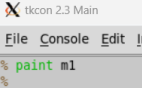
To begin we now connected the transistors in an inverter fashion. Since the transistors are symmetric devices we can just draw a connection across to connect the drain of the nmos to the source of the pmos. We do so by drawing a box overlapping the two vias, and then calling "paint m1" in the below fashion.
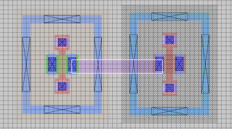
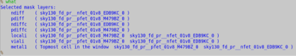
Now that we have created a wire connection, it is helpful to know how to remove wire connections. Crucially, in the cell hierarchy, lower cells have their layers locked by default, so any action taken to modify the layout will only affect the top level cell. Thus we can call "erase" or "erase x" where x is the specific layer to erase. This will erase what is currently under the white box. Along with this information, another key aspect of drawing your wire connections is making sure that what you are purposefully connecting is not actually shorting to any other net. To check if you are shorting a net you place your mouse over the wire and then repeatedly press "S", this flashes that net and highlights everylayer that is connected to where you pressed "S". Doing this also allows you to check what layers are there by running the command "what" From here we will finish the design of the inverter.
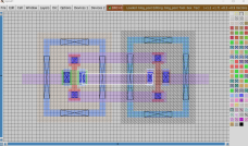
As can be seen, the output line of the inverter has been flashed and the "what" command has been run. Along with this we can see that the DRC errors have been fixed as the added m1 layers satisfied the minimum width/area error.
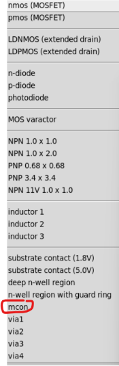
While the transistor terminals have been added, the bulk connections have not. To do this we add two vias, one on both sides connecting to the auto generated guard ring. This is done by boxing over the light blue and purple and going to Device 1 and pressingmcon.
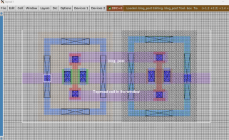
This connects the bulk to the GND and VDD inputs respectively. Also, depending mcon only drills down from metal1 to the local interconnect layer. The guard ring here is what vias into the bulk.
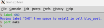
From here we have the wire connections, but for this layout to fully be done we must finish the last step, Layout Versus Schematic. To do this step we need to do three more things, add port labels into Magic, generate the spice netlist, and generate the schematic netlist. For the Magic component we again place the box over the m1 layers and type "label X" where X is the name of the port, and then "port make" to make the label into an actual port. This will make a blue box where the white one was.

From here we add all of the ports to the layout and run the Magic extraction, to get the netlist through the following commands:
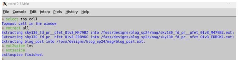
Select top cell, selects the top cell. Extract all, creates an extraction file of the layout which is then used by ext2spice to generate the netlist. "Ext2spice lvs" sets up the ext2spice command to generate a spice netlist in the NGspice format. The final command runs ext2spice and generates the netlist.
From here we go to xschem to generate the needed schematic netlist. Once that is done, we open up Netgen and compare the two netlists in the following way:

Here the "lvs" command is being called on two spice files demarcated by the curly braces "{}"". The spice file is listed first and then the subcircuit inside the spice files that you wish to compare. The file path listed above is for my Docker setup and your file path may be different. The final item typed out is the file path to the technology file that actually allows netgen to understand what each item in the netlist is. Once that is typed out and run you should get this:
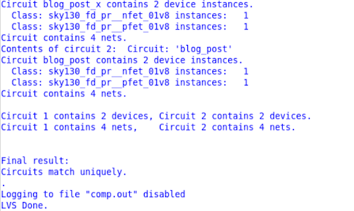
This outputs a detailed report of the LVS command that either tells you the netlists match or that it failed. In this case the netlists match and we did indeed create an inverter. The next step is to then re-extract the layout to run an extracted simulation. Since we set ext2spice up with lvs, that generated spice file has no indication of any resistances or capacitance. Thus we run another set of commands to get the full parasitic extraction. We run:
"flatten blog_post_flat
load blog_post_flat
cellname delete blog_post
cellname rename blog_post_flat blog_post
select top cell
extract do local
extract all
ext2sim labels on
ext2sim
extresist tolerance 10
extresist
ext2spice lvs
ext2spice thresh 0
ext2spice extresist on
ext2spice"
These commands runs and produces a parasitic netlist full with resistances and capacitances. This command run requires that the layout be flattened, ie no cell hierarchy, this is not ideal for layouting, so before this command is run, copy and save a non flattened version somewhere else.
There it is, a quick tutorial on how to do layout in Magic. As with everything more can be said and be found from Magic's own website found here. I hope the tutorial was helpful and I hope you enjoy your time laying out integrated circuits as the scale goes from 2 transistors to thousands.