Making Chips is NOT Easy
Angela Cui and Tomas Choi
March 3rd, 2024
Intro to Design for Test
Throughout the design of various IP blocks, we always test. We check that the design meets the specified requirements and behaves as intended under various conditions. We put the IP blocks through a series of simulations that check that the design passes common cases and stress cases. Each design has to be able to reliably handle the typical, expected scenarios they will encounter during normal operation. Hardware needs to also pass stress tests to ensure it can operate reliably under more extreme conditions. The stress tests, in our case, can come in the form of specific data values or different input and output delays. To ensure coverage of a large number of possibilities, we simulate the design with manually determined and random data. Before we send our chip to fabrication, we test ... A LOT.
Then, if we are testing so much, is there a possibility that the chip doesn't work when it comes back to us? Unfortunately, yes. There are a few reasons why this could happen. The fabrication process, while highly sophisticated, is not perfect, so there can be manufacturing defects. Variabilities in many different factors can introduce defects such as shorts, opens, or variations in transistor sizes, which can affect the performance of the integrated circuit or cause it to fail completely. Throughout the packaging and assembly process, more issues could arise that can lead to failures due to mechanical, thermal, and electrical stress. Additionally, no matter how thorough our testing strategy was during our design stage, it is impossible to account for every possible scenario that the design might undergo. There are certain unforeseen conditions that only become apparent once the design is fabricated.
Nevertheless, learning from these failures that come after fabrication becomes very useful to us as we work on future designs. It is key that we are able to identify which part of the chip is failing and have a sense of why this is the case. The chips are very expensive and they take a long time to design and fabricate, so the time and cost factors that come out of this process make it crucial that we are not just looking at the whole chip as a black box and have no idea what the problem might be. This is why we have Design for Test.
Design for Test (DFT) is a technique to add testing features in the hardware that enable for easier debuggability of the design. This way any defects that come out of the manufacturing process can be identified efficiently. Implementing DFT in designs is a balance between increasing the testability and diagnosability of the chip and managing the trade-offs in terms of additional silicon area, power consumption, and potential impacts on the chip's performance.
DFT techniques
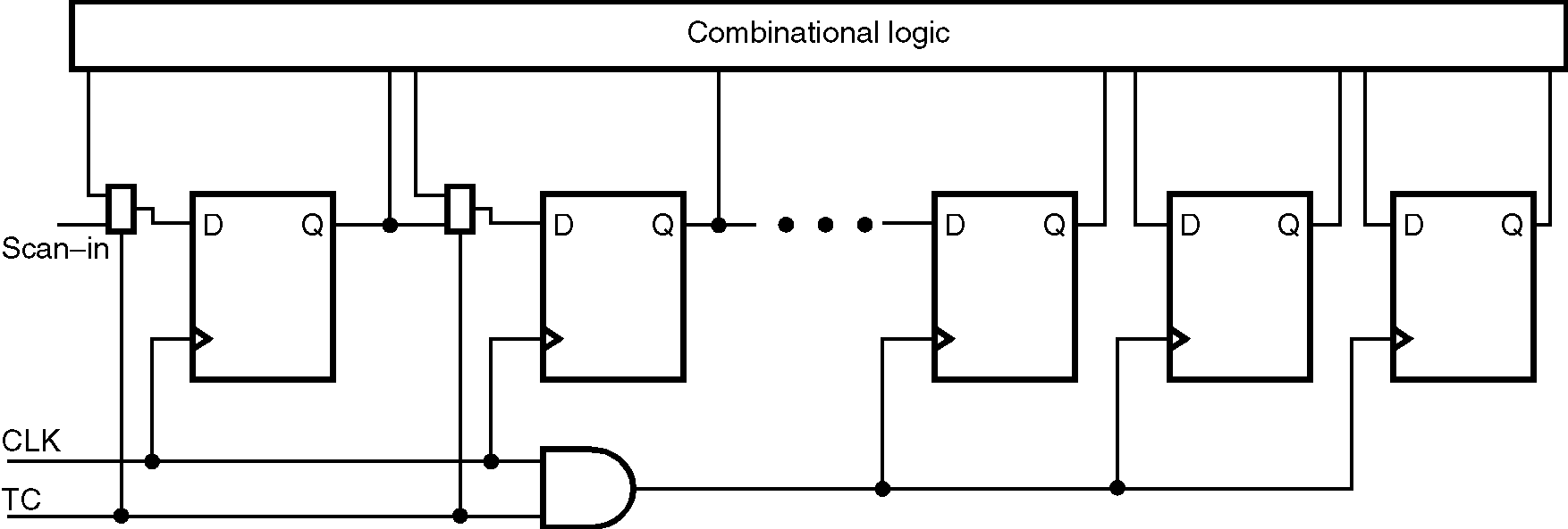
There are two fundamental DFT techniques: scan design and built-in self test. Scan design works by incorporating a series of flip-flops across the design, allowing the insertion of input values and the capture of output values. This enables the testing of the different modules in our design. There are a few steps to testing using the scan design. First, the IC is placed in test mode, and the test vectors are loaded into the scan chains, setting the internal states of the circuit to the desired test conditions. When the chip starts doing work, it will output values into the next flip-flop in the chain, making it possible to capture those test responses for analysis. Those outputs can be compared to the expected results to identify differences that might be causing the issue in the whole design. The core idea behind scan design is to make testing more manageable and efficient by enhancing their controllability and observability.
Built-in self test is a technique that allows an IC design to essentially test itself. There are two major types of built-in self test: memory built-in self test and logic built-in self test. Memory built-in self test tests memory units by generating patterns that are stored in memory, then loading from those memory cells to check for any inconsistencies. Logic built-in self tests use a pseudo random pattern generator as an input to a block on the IC. The output is then checked for correctness, typically by compressing the results into a signature and checking them against a register that stores the correct signature. Typically, built-in self tests are implemented to meet design constraints such as low cost for testing, limited access to technicians once an IC has been employed, and high reliability. Thus, although built-in self tests may incur additional area and energy overhead to an ASIC design, they are highly effective in reducing test-cycle duration and test setup complexity.
Digital System Overview
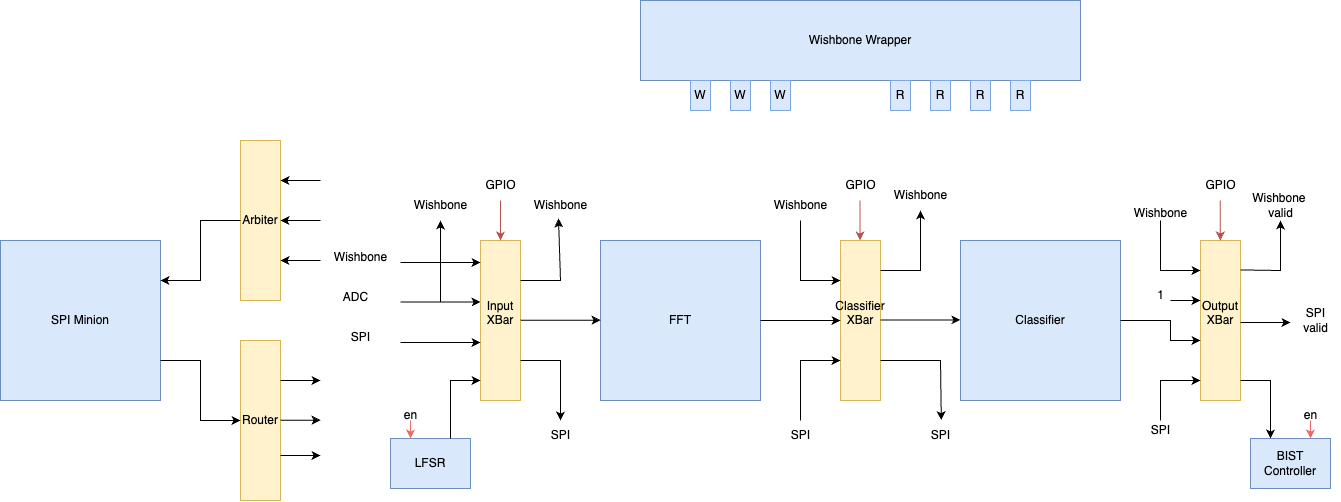
Last year, the digital subteam taped out a FFT with an SPI interface. This year, we are adding functionality for the design to communicate with the on-chip RISC-V processor. The FFT will take inputs from the analog subteam's ADC and output them to a custom classifier. The classifier classifies whether the data is a bird call and signifies to the processor through the wishbone bus if the ADC data is valid based on the classification. The RISC-V processor will then further process the data. The aim of the on-chip classifier is to save energy by only having the processor do work for a given piece of data if it is a bird call.
A significant concern when it comes to IC system design is what would we do if a certain part of our chip malfunctions post-silicon and how to test our chip. Unlike breadboarding or software testing, we can not probe a signal or print out a variable if our chip does not behave as we expect. So, we apply the concepts mentioned earlier to ensure that we can comprehensively test our physical chip.
Our chip takes inputs through SPI, wishbone, or the ADC, ensuring that we have backups if any one interface is buggy. Similarly, our chip can send outputs through SPI or wishbone. Similar to the scan design concept, we add functionality to probe the FFT module or the classifier module using the crossbars. Each crossbar is configurable using a set of GPIO pins, allowing us to configure the chip without having to hook it up to SPI or flash code over wishbone.
We also add in built-in self test capability to the system using a pseudo-random number generator with a preset seed, implemented as a linear feedback shift register, as the input to the FFT. The output of the classifier is then compared to a signature register using a BIST controller, which toggles a GPIO pin if the outputs match. The idea is to comprehensively test the system and each module through either the wishbone or the crossbar. Then, if we wish to quickly check for functionality across different chips or at startup, we can use the BIST for fast automated testing.