Bridging Two Worlds: Analog-to-Digital Converters
David Bertuch and Jon Ho
March 29rd, 2024
ADCs serve as a bridge between the natural world (where signals occur in continuous time) and the digital domain (where signals occur in discrete time, with discrete amplitudes). They are an essential part of any sensing front-end, and will only grow in relevance with the continued deployment of edge-computing solutions as well as the continued push to place ADCs closer and closer to the front of the signal chain. This year, the analog subteam is taping-out two types of ADCs (flash and delta-sigma) in an effort to satisfy the needs of our campus partner, who requires a system that can convert the audio signals produced by a microphone into digital data. In this blog post, our goal is to provide a high-level overview of the three fundamental types of ADCs (delta-sigma, SAR, and flash) that exist and share our personal experiences designing delta-sigma and flash ADCs for the very first time.
Delta-Sigma ADCs:
Delta-Sigma ADCs offer high-resolution, low-noise conversion with a relatively small footprint. The topology of these circuits causes them to convert slower than other available ADC designs, but their numerous benefits make them a popular choice in many circuits. These ADCs use high-frequency oversampling in a feedback loop to modulate analog signals into a digital bit stream. This digital output is then fed into a digital filter, which obtains the signal in the frequency band of interest. Finally, a decimator is used to down-sample the high-frequency bit stream into a useful, high- resolution digital signal.
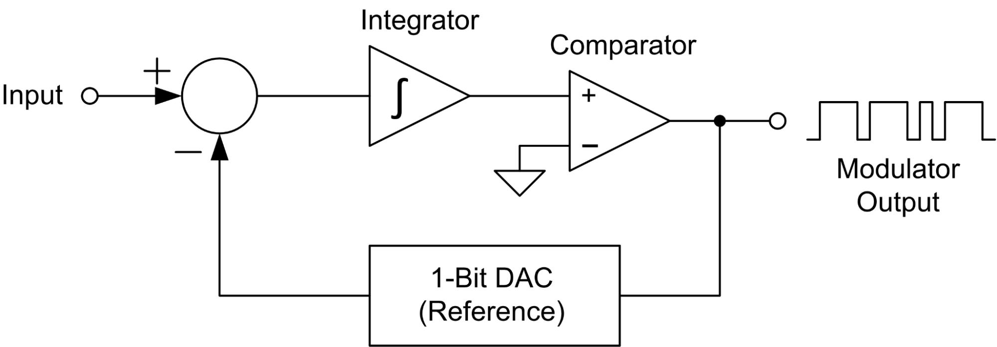
Block Diagram of a First-Order Delta-Sigma ADC Modulator [1]
The front-end of the ADC, the modulator, is the heart of the Delta-Sigma. In a first-order design, as seen in Figure 1, the difference (delta) between the input analog signal and the digital feedback is fed into an integrator (sigma). The resistor and capacitor used in the integrator dictate the frequency cutoff of the modulator. The integrator then feeds into a clocked comparator. On every clock cycle of the oversampling frequency, the integrator signal is compared with the mid-rail voltage to produce a logical 1 or 0 on the digital output. The 1-bit DAC effectively acts as a level shifter to convert the logical output into voltages that are appropriate for the input signal amplitude.
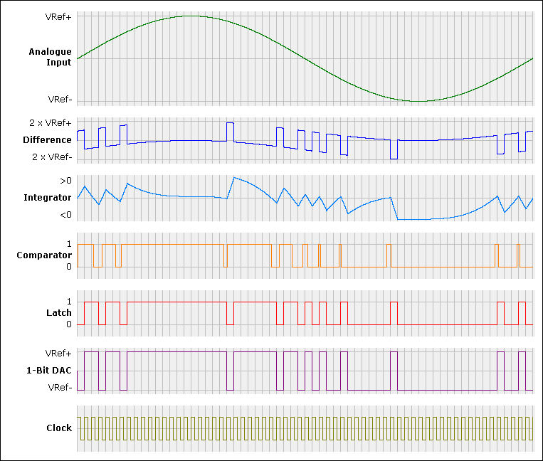
Waveforms of a Delta-Sigma Modulator [2]
The "Latch" wave in Figure 2 represents the desired output of the modulator. As the analog input rises in amplitude, the latch output spends more time as a 1. Conversely, as the input signal falls low, the latch output is favored toward 0. By averaging the digital signal, we can reconstruct the waveform of the analog input.
One of the primary appeals of the Delta-Sigma modulator is its noise-shaping ability. All ADCs face a problem called "quantization noise." Since analog signals are continuous in time, while digital signals are discrete, there will be instances in which the analog input differs from the digital approximation. This difference is referred to as "noise." Due to the oversampling rate of the Delta-Sigma, this noise is flattened across a greater frequency range, which is also pushed to higher frequencies by the high-pass filter effects on the noise. These effects can be visualized in Figure 3.
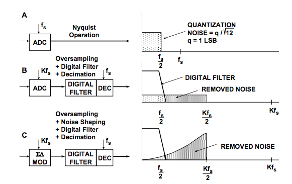
Noise Profile of a Nyquist ADC (a), an ADC with Oversampling and Filtering (b), and a Delta-Sigma ADC (c). [3]
By incorporating additional differentiation and integration stages, we can enhance the noise shaping ability of the ADC. Figure 4 illustrates the noise profiles of higher-order modulators. Increasing the modulation order and employing a larger oversampling ratio allows us to boost the effective bit resolution of the ADC. We intend to tape out a second-order ADC modulator this Spring, depicted in Figure 5. This design aims to achieve an effective output of 8 1/2 bits.
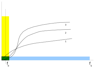
Signal Band of Interest (in yellow) and the Noise Profiles of Delta-Sigma ADCs of Various Orders. [4]
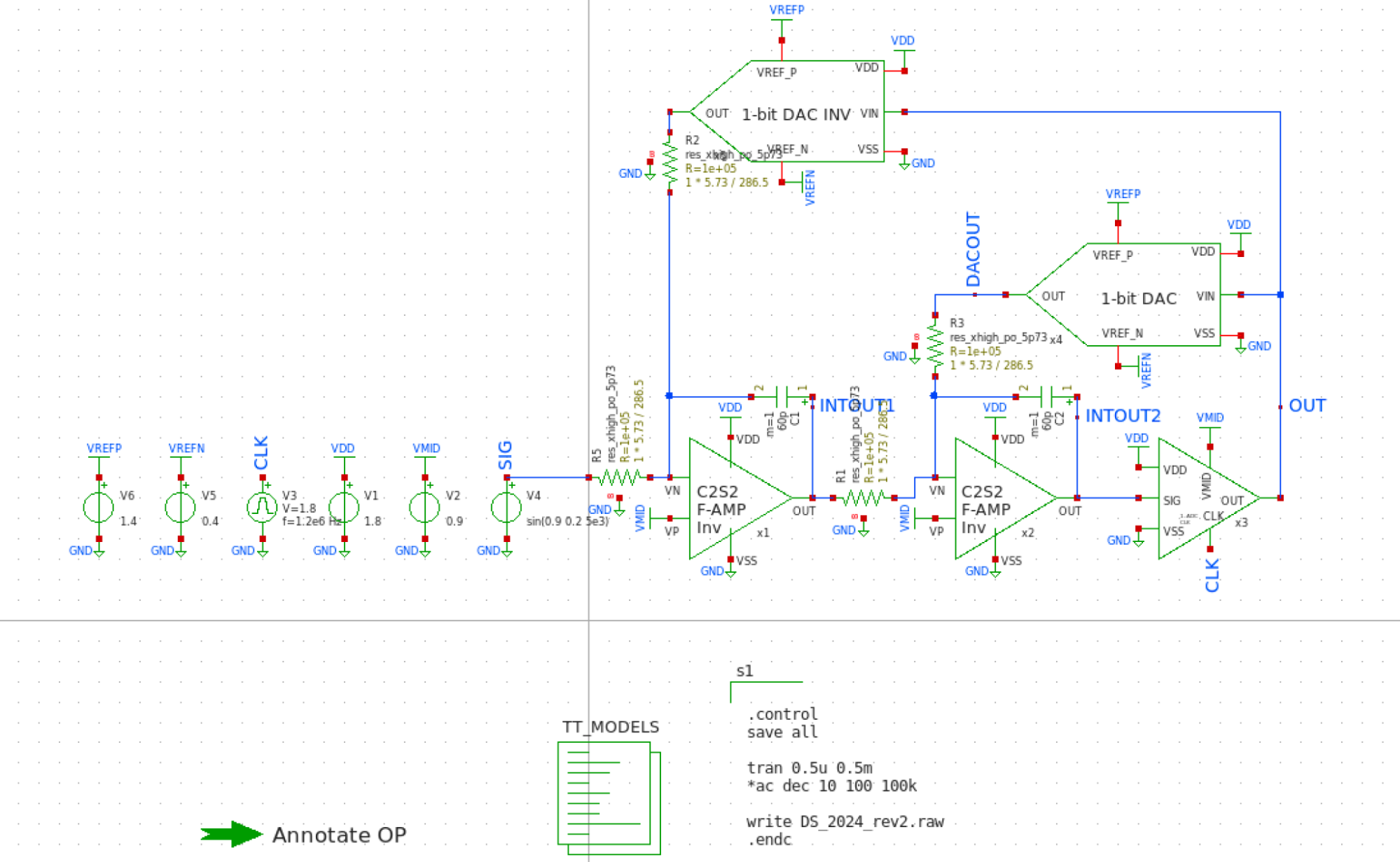
Schematic of C2S2 Second-Order Delta-Sigma Modulator.
Successive Approximation ADCs (SAR):
SAR ADCs are the most popular type of ADC when it comes to data-acquisition. They typically have resolutions ranging between 8 to 18 bits and sampling rates of a few MHz. As shown in Figure 6, the signal is first fed into a sample-and-hold circuit during the acquisition phase.The sample-and-hold circuit could be as simple as a switch followed by a RC circuit: 1) during acquisition, the switch is closed and the capacitor charges 2) during conversion, the switch opens and the voltage is stored on the capacitor.
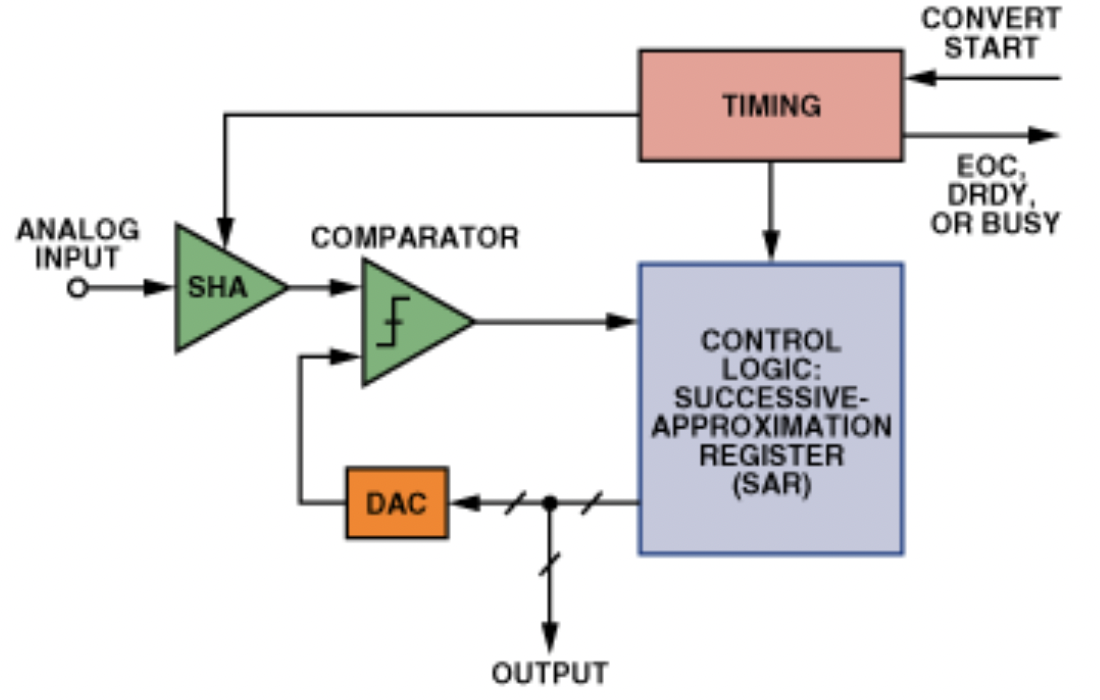
Block Diagram of a Basic SAR ADC [5]
During the actual conversion period itself, the DAC is initially set to mid-scale (MSB is set to 1, and the remaining bits are 0) and the comparator determines whether the sampled voltage is higher or lower than the mid-scale voltage. If the input voltage is indeed higher, then the MSB is kept as a 1; if not, the MSB is set to 0. Based on the outcome of this initial comparison, the DAC is then set to 1/4 scale or 3/4 scale - and the process continues. Fundamentally, the SAR ADC implements a binary search. Though this form of successive approximation allows SAR ADCs to achieve good accuracy, there is a significant trade off in speed as N-bit SAR ADCs typically require N conversion periods before another value can be sampled.
Regarding the comparator, this block is typically designed to have an input referred noise that is lower than 1 LSB. The comparator's ability to resolve small voltage differences limits the overall accuracy of the system. Furthermore, the time it takes to resolve small voltage differences also limits the speed of a SAR ADC. One can imagine that a differential-pair-based comparator can resolve large voltage differences faster than small voltage differences since the former produces a significantly larger differential current than the latter.
Regarding the DAC, this block is typically implemented using a bank of capacitors that are binary-weighted in value (a N-bit SAR ADC will have N binary-weighted caps and an additional cap for the dummy LSB). Though the use of unit capacitors can help with matching, capacitive DACs typically require calibration schemes. It is also worth noting that the setting time of the DAC also limits the speed of the SAR ADC.
With all of these considerations in mind, it is not surprising that SAR ADCs are the go-to option in power-limited, area-limited applications. Fundamentally, SAR ADCs trade speed for resolution (and area). In retrospect, the analog sub-team should likely have designed a SAR ADC given the low-power, area-constrained nature of the bird-tag project (a potential project for next year!).
Flash ADCs:
Flash ADCs are perhaps the simplest and certainly the fastest type of ADC available. As shown in Figure 7, a simple N-bit flash ADC consists of 2 N equally-sized resistors (placed in a resistive ladder); 2 N parallel comparators; and a priority encoder. Each of the comparators compares the input signal against an equally-spaced reference voltage (a single voltage increment is equivalent to 1 LSB).
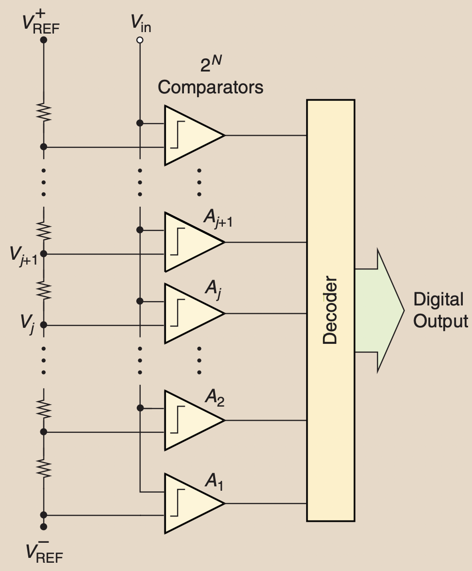
Block Diagram of a Basic Flash ADC [6]
Based on the parallel nature of the architecture, we know the flash ADC is faster than typical delta-sigma and SAR ADCs. As compared to the SAR ADC that requires N comparison cycles, the flash ADC performs all of its voltage comparisons in parallel - and importantly, in a single cycle. That being said, it is also obvious that flash ADCs do not scale well due to the exponential nature of the required number of comparators and resistors (poor area and power scaling). Furthermore, this architecture exacerbates issues associated with mismatch and process variation. With these considerations in mind, it is not surprising that flash ADCs are typically limited to resolutions of 4 to 8 bits (with sampling rates reaching into the GHz range).
To ease the power-speed tradeoff, comparators that consume zero static power can be utilized. One popular example of this would be the strongARM comparator, as shown in Figure 8. At a high level, the strongARM comparator is a dynamic, latched comparator. When CLK is low, the circuit pre-charges the output nodes (as well as various internal nodes to VDD). When CLK is high, the tail current transistor turns on; the differential pair generates a differential current; and the cross-coupled structures help pull the outputs to opposing rails (regeneration). One important thing to note about the strongARM comparator is that the threshold voltage of the input pair limits the full-scale voltage of the flash ADC. In other words, the common-mode voltage of the input signal lie above the input pair's threshold voltages since these devices must turn on in order to generate differential currents.
A Basic strongARM Comparator
Additionally, the strongARM comparator suffers from kick-back noise. During regeneration, large transient currents are drawn by the circuit. These currents couple back to the inputs through the parasitic Cgs and Cgd capacitors in MOSFET devices. In Figure 9, we show the effects of kick-back in a strongARM comparator circuit that we personally designed.
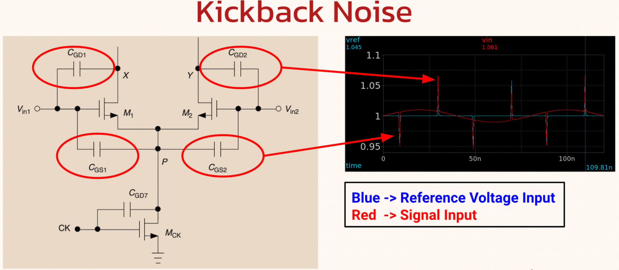
Kick-back from a strongARM Comparator
The effects of kickback can be mitigated through the use of a pre-amplifier. The pre- amplifier acts as a buffer and lowers the input-referred kick-back noise by a factor equal to its gain. In Figure 10, we show a simple pre-amplifier that we designed. In Figure 11, we show how the aforementioned pre-amplifier reduces the kick-back noise generated by our strongARM comparator. However, it is important to note that our pre-amplifiers increase static power consumption (due to the amplifier's use of a tail-current transistor for current biasing) as well as overall area.
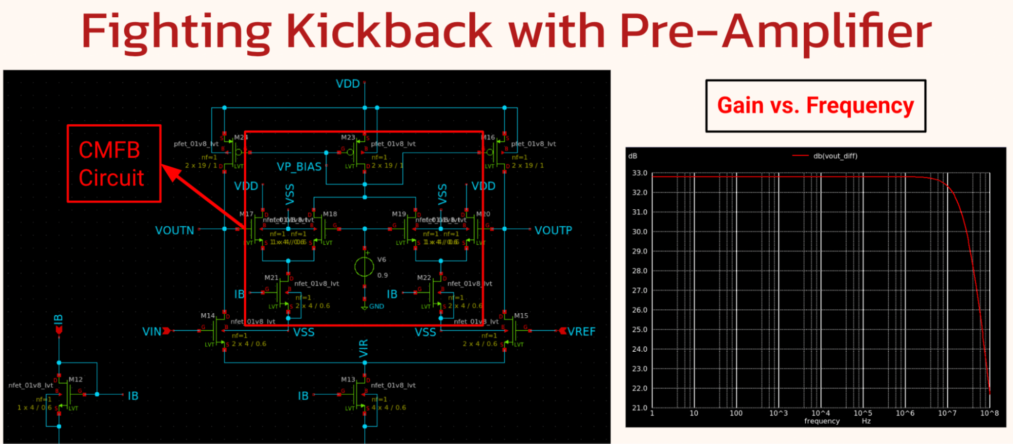
A Simple Pre-Amplifier
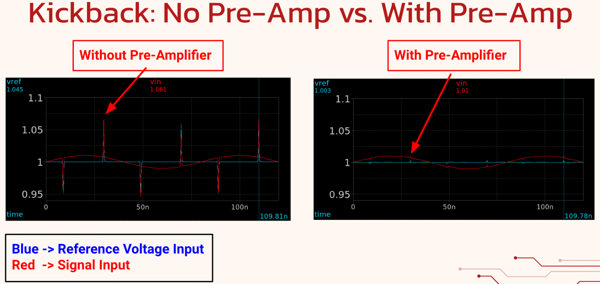
Pre-Amps Reduce Kick-Back
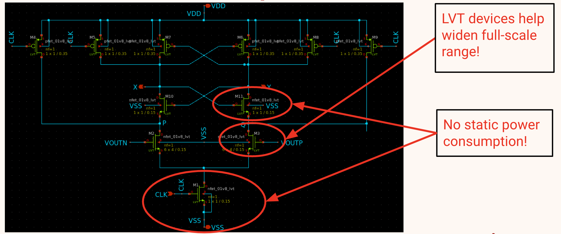
In the end, our team actually opted to use a low kick-back, class AB comparator. This type of latched comparator is similar to the strongARM comparator in the sense that it also leverages cross-coupled structures for regeneration. As shown in Figure 12, our low kick-back comparator has two transistors (M14 and M9) that essentially decouple the input differential pair from the regenerative nodes. Furthermore, the use of cross- coupled MOSCAPs helps neutralize unwanted current.
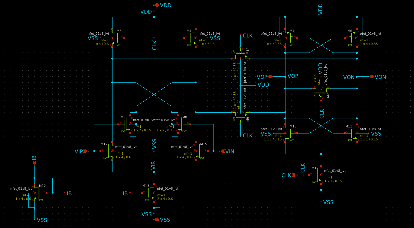
Kick-back Optimized Class AB Comparator
Backing out to the system level, our team opted to design a 4-bit flash ADC. Initially, we were shooting for 5 to 6 bits. However, due to a lack of trust in Sky130's models, we were not confident if the provided mismatch parameters were accurate (Pelgrom's law). Hence, we selected 4-bits to be safe and increased the size of the input differential pair devices (in the comparators) to lower input-referred offset voltages. Furthermore, as shown in Figure 13, our flash ADC uses small resistor values in the resistive ladder to lower the impedance of those nodes and hence render those nodes less sensitive to kick-back (we used parallel segments to increase the area of the resistors to help with better matching). Additionally, one of our team member's designed optimized RS- latches that follow the output of the comparators. And lastly, one of our team's members designed the 16:4 priority encoder using Sky130's provided standard cells. The design is able to sample at frequencies above 25MHz whilst driving 20pF loads.
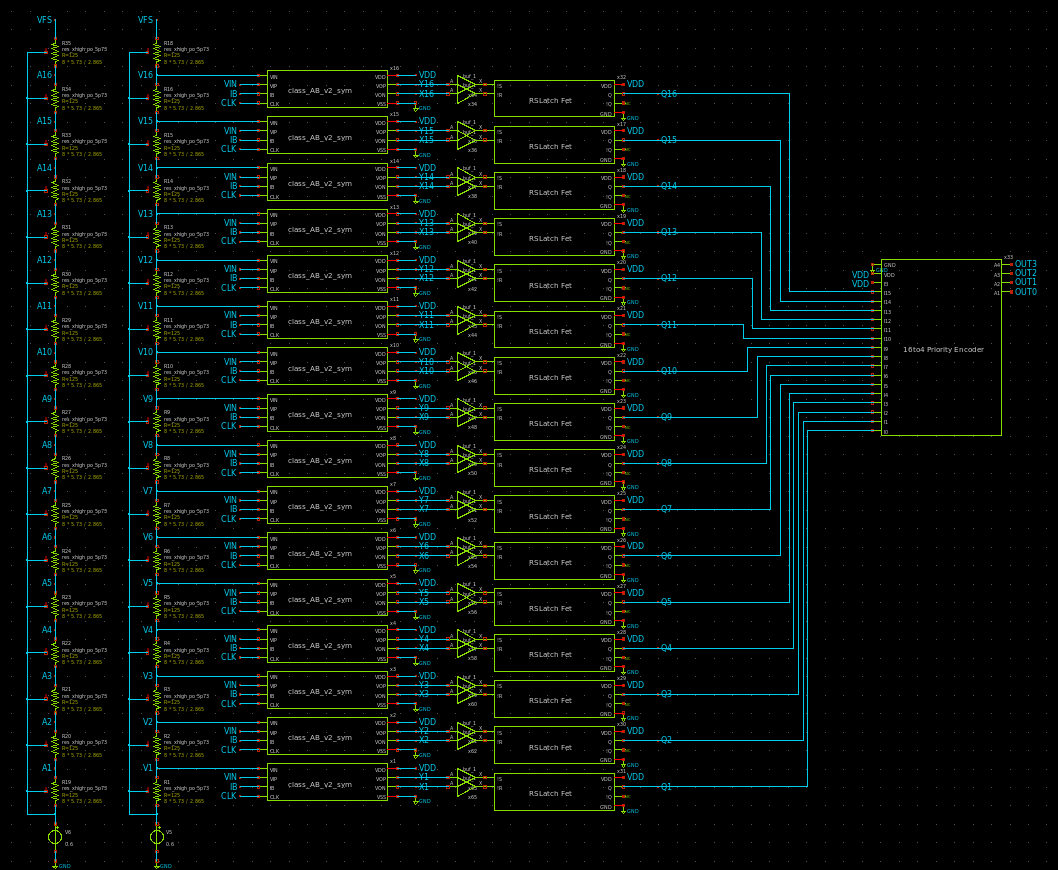
From left to right, the flash ADC uses a resistive divider; kick-back optimized class AB comparators; buffers for electrical isolation; RS latches, and a 16:4 priority encoder.
Conclusion:
In engineering design, selecting the optimal ADC often hinges on the specific requirements of the application, rather than a one-size-fits-all solution. When prioritizing low noise and high resolution, the Delta Sigma ADC stands out as an excellent choice. For applications where power efficiency is paramount, the SAR ADC proves to be advantageous. On the other hand, if speed is a critical factor, opting for the flash ADC is a reliable approach. Ultimately, the best ADC selection depends on carefully weighing the unique needs and priorities of the given project. We hope that this post provides valuable insight into the realm of analog-to-digital converters!
References:
[1] Delta Sigma ADC Basics: Understanding the Delta Sigma Modulator
[3] Understanding and designing sigma-delta A/D converters
[4] How to plot noise-shaped spectrum of first-order incremental sigma-delta ADCs?
[5] Which ADC Architecture Is Right for Your Application? | Analog Devices
[6] BRSummer17FlashADC.pdf (ucla.edu)
Thumbnail: Wikipedia